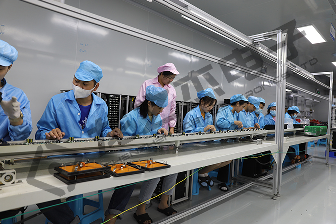
What is DIP?

In PCB assembly, DIP and SMT are often mentioned, which may be difficult for newcomers to the industry to understand. Actually, DIP and SMT are both process methods for integrating electronic components on a PCB. SMT is a surface mount technology that does not require drilling and is currently the most popular process in the PCB industry. However, when encountering electronic components that are too large in size, SMT is not applicable, and DIP is required.
DIP is an important part of the PCBA production process, which has two implementation methods: manual insertion and machine insertion. Currently, manual insertion is the main method. The DIP process generally involves shaping electronic components, and then manually or robotically inserting them onto the PCB. After insertion, the board undergoes wave soldering, and once the soldering is complete and the components are fixed in place, the board is trimmed to the appropriate size. After construction, the board is inspected, and if incomplete soldering is found, touch-up soldering is required. Once touch-up soldering is complete, the PCBA board must be cleaned. After completing these steps, functional testing can be performed, and if there are no issues, the board can be packaged and shipped.
When encountering larger electronic components or boards that are not suitable for SMT, DIP is necessary for PCBA processing. In addition, because the process methods for SMT and DIP are different, their testing methods also differ, and each has its own system. Although SMT is currently the mainstream process for PCBA production, DIP still has its place and cannot be replaced.

