
What Is the Half-Hole Process?
As electronic products continue to pursue higher performance and smaller form factors, the requirements for PCB assembly and inter-board connections have become increasingly demanding. To integrate more functions within limited space, many products have adopted modular or “daughterboard–motherboard” designs, making the connection method between boards especially critical. While traditional connectors or flex cables are common solutions, they are not ideal in tightly packed layouts or cost-sensitive applications. Under these conditions, the half-hole process (Half-hole / Castellated Hole) has emerged as a solution that balances space, cost, and reliability, and is now widely used for soldering modules to main boards.
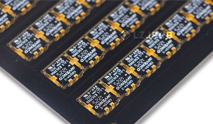
The hallmark of the half-hole process is designing plated through holes along the edge of the PCB. After routing and profiling, these holes are cut in half, leaving “semi-plated holes” with fully intact copper on the hole walls. Despite being partially removed, the plated walls still allow the feature to function like a surface-mount pad during soldering. When a daughterboard is soldered to a motherboard through half-holes, the two PCBs achieve both reliable electrical connection and solid mechanical support. Thanks to its compact structure, this method is particularly well-suited for space-constrained electronic products and helps enable modular system layouts.
Compared with traditional connection methods, the half-hole process offers several significant advantages. First, it greatly saves space by eliminating the need for additional connectors, making it ideal for low-profile devices and perfectly suited for compact daughterboard–motherboard PCB architectures. Second, the half-hole approach reduces material costs and assembly steps, improving production efficiency—especially in designs where the daughterboard is soldered onto the motherboard like a surface-mount component. In addition, half-hole solder joints provide strong mechanical retention and excellent electrical conductivity, ensuring high reliability for communication modules, industrial control boards, and customized functional daughterboards that operate over long periods. This is why WiFi/Bluetooth modules, power conversion modules, sensor boards, and various embedded expansion boards commonly adopt half-hole pads as standard interfaces, enabling simpler, more efficient, and more durable connections between PCBs.
As the electronics industry continues to evolve toward higher density, greater functionality, and further miniaturization, the half-hole process will play an increasingly important role in PCB assembly. It offers a flexible, stable, and cost-effective connection method, bringing more possibilities to product structural design and manufacturing processes, and has become an indispensable technique in modern PCB manufacturing.