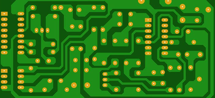
Introduction to PCB Blind and Buried Via Technology.

In PCB manufacturing, buried vias are an essential process that plays a critical role in specific electronic devices and products. This article will delve into the concept of PCB buried vias, the manufacturing process, and their applications in electronic devices.
The Concept of PCB Buried Vias
Buried vias refer to blind vias located within the PCB, connecting different layers. Blind vias are holes that do not penetrate the entire PCB; they only connect a portion of the board and do not appear on the surface. In contrast, buried vias are internal connections within the PCB layers and are not visible from the outside of the board. Buried vias are commonly used in the production of multi-layer PCBs, especially for complex circuits and high-density interconnect (HDI) board designs, providing more routing space and design flexibility.
The Manufacturing Process of PCB Buried Vias
The manufacturing process of PCB buried vias is relatively complex and typically involves the following steps:
1. Layer Stacking Design:
During the PCB design process, the required number of layers and locations for buried vias are determined, and the corresponding layer stacking design is implemented. Buried vias usually appear in internal layers, connecting different circuit layers.
2. Laser Drilling:
Laser drilling technology is employed to create blind vias within the internal layers of the PCB. Laser drilling allows for high precision and efficiency, ensuring the quality and accuracy of buried vias.
3. Via Filling:
After drilling, the buried vias need to be filled. Typically, conductive paste or conductive material is coated within the buried vias to achieve interconnections between different layers.
4. Lamination:
Following the via filling process, the multi-layer PCB is laminated to create reliable connections between the layers.
Applications of PCB Buried Vias
PCB buried vias find widespread applications in electronic devices. They are commonly used in the design of complex circuits and HDI boards to meet the demands for increased signal transmission and power requirements. Some common applications include:
1. High-Performance Computers:
Buried vias facilitate connections and communication between complex internal circuits in high-performance computers.
2. Communication Equipment:
Buried vias enable high-frequency signal transmission and connections in communication equipment, enhancing the efficiency of devices.
3. Industrial Controllers:
For industrial controllers and similar devices, buried vias offer more routing space and signal transmission paths, resulting in increased flexibility and reliability.
Conclusion
PCB buried vias are a crucial manufacturing process in modern electronics, playing a pivotal role in the design of complex circuits and HDI boards. By providing internal connections within PCB layers, buried vias offer greater design flexibility and reliability. They are indispensable components in various high-performance electronic devices, ensuring their proper functioning and exceptional performance.

