What is the pcb pad?

I. Definition of PCB Solder Pads
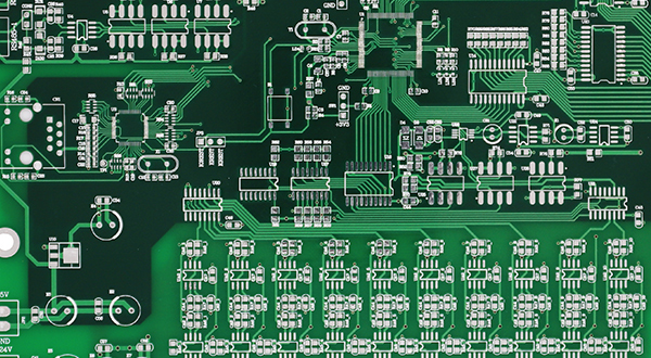
PCB solder pads are metal pads on a printed circuit board that connect the pins of the components and the circuit board. Solder pads are usually made of copper and coated with a surface treatment for easy soldering. The size, shape, and arrangement of the solder pads depend on the pin layout and size of the components on the circuit board. During the assembly process, the solder pads connect the components on the circuit board through soldering to achieve electrical connection.
II. Types of PCB Solder Pads
Based on the different soldering methods, PCB solder pads can be divided into two types: surface mount pads and through-hole pads.
Surface Mount Pads
Surface mount pads achieve electrical connection by soldering the pins of the components directly onto the pads on the surface of the circuit board. Surface mount pads are usually rectangular or square, with sizes and shapes that match the pin layout and size of the components. The advantages of surface mount pads are high-density layout, which saves circuit board space, and improved reliability and anti-interference capabilities.
Through-Hole Pads
Through-hole pads achieve electrical connection by inserting the pins of the components into the holes on the circuit board and connecting the pads inside the holes with the pins through soldering. The size and shape of through-hole pads usually match the pin layout and size of the components. Through-hole pads can withstand larger currents and power, making them suitable for components that require high current and power.
III. Manufacturing Processes of PCB Solder Pads
The manufacturing processes of PCB solder pads typically include the following steps:
Copper Foil Coverage: Cover the positions of the solder pads on the circuit board with a layer of copper foil, typically by chemical or mechanical copper foil coverage.
Pattern Making: Use photolithography to draw the pattern of the solder pads on the copper foil.
Etching: Etch away the unwanted copper foil, leaving only the pattern of the solder pads.
Cleaning: Chemically clean away the debris and dirt generated during etching.
Soldering Surface Treatment: To improve soldering quality, a layer of soldering surface treatment material, such as HASL, ENIG, or OSP, is coated on the surface of the solder pads.
IV. Common Problems and Solutions
During the manufacturing and assembly process of PCB solder pads, some common problems may occur, such as solder pad short, open, and void. Here are some common problems and solutions:
Solder Pad Short: It may be caused by a small distance between the solder pads or overheating during soldering. The solution is to adjust the solder pad layout or control the soldering temperature.
Solder Pad Open: It may be caused by poor contact between the solder pad and the component pin or insufficient temperature during soldering. The solution is to increase the soldering temperature or adjust the soldering time.
Solder Pad Void: It may be caused by poor soldering surface treatment or uneven temperature during soldering. The solution is to replace the soldering surface treatment material or adjust the soldering temperature.
In summary, PCB solder pads are essential components in the circuit board assembly process. Understanding the types, manufacturing processes, and common problems and solutions related to PCB solder pads can improve the quality and efficiency of circuit board assembly.

