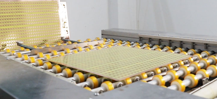
Unveiling the Purpose of PCB Etching

1.Defining Circuit Patterns
PCB etching is responsible for defining intricate circuit patterns on the board's copper layers. Through a chemical or mechanical etching process, excess copper is selectively removed to create conductive pathways that form the desired circuitry. This precise and controlled etching ensures the accurate transmission of electrical signals and enhances the overall functionality of the circuit board.
2.Removing Excess Copper
During the PCB fabrication process, copper is initially deposited on the substrate to create the conductive pathways. However, this deposition often results in the presence of unwanted copper traces that need to be eliminated. PCB etching allows for the precise removal of excess copper, leaving behind only the required circuit patterns. This controlled removal ensures the optimal performance of the circuit board while minimizing the risk of short circuits or signal interference.
3.Creating Isolation Between Traces
In complex circuit boards with multiple layers and densely packed components, it is vital to maintain proper isolation between adjacent traces. PCB etching plays a critical role in creating the necessary gaps or isolation areas between traces to prevent unintended electrical connections. This process ensures the integrity and reliability of the circuitry by eliminating the possibility of cross-talk, signal interference, or short circuits that can compromise the overall functionality of the board.
By understanding the purpose and significance of PCB etching, engineers and manufacturers can make informed decisions during the design and manufacturing stages, leading to the production of high-quality circuit boards that meet stringent performance requirements. In the subsequent sections, we will explore the various etching methods, considerations, and advancements in PCB etching technology, providing valuable insights into this essential manufacturing process.

