
What Are the Common PCB Via Processing Methods?
In the PCB manufacturing process, vias play a crucial role as bridges that connect signal or power traces between different circuit layers. To meet the requirements of electrical performance, solderability, reliability, and manufacturing processes in various application scenarios, vias often need to undergo specific treatments during PCB fabrication. This article introduces three common via processing methods: via tenting, via plugging, and via covering.
To understand these via processing methods, we first need to understand what a via is. A via is a plated hole on a PCB used to electrically connect different circuit layers. In addition to establishing connections, vias can also assist with heat dissipation. There are three main types of vias: through-holes, blind vias, and buried vias. Via processing usually refers to the treatment of through-holes, as blind vias and especially buried vias typically do not require surface-level processing.
It’s also important to note that PCBs include a solder mask layer, and via processing is closely related to this layer. Since most via processing involves operations on the solder mask, understanding its role helps clarify these treatment methods.
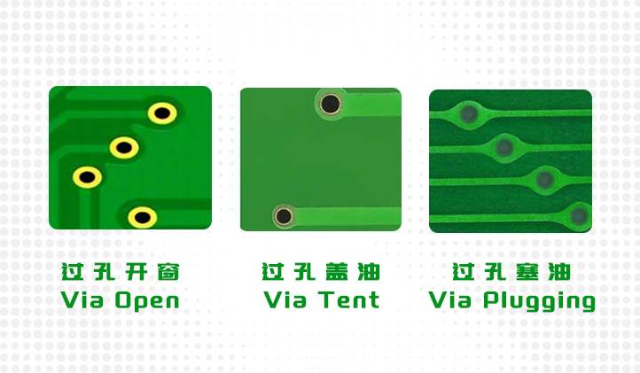
1, Open Via (Solder Mask Opening):
An open via refers to a via where the solder mask is intentionally not applied, leaving the via fully exposed. This approach is mainly used to facilitate heat dissipation, allow electrical contact, or serve as a test point. The via is neither filled nor covered.
2, Via Plugging (Filled Via):
Via plugging involves completely filling the via with specially formulated ink or resin, typically using a vacuum or screen printing process. This treatment enhances the mechanical strength and sealing of the via, helping to prevent solder or flux from penetrating the hole during assembly.
3, Via Tenting (Covered Via):
Via tenting refers to applying solder mask over the via without filling it. The mask simply covers the via pad and hole, hiding it from the surface. This is mainly used to prevent contamination from solder, dust, or flux, and to protect the via from environmental factors. Tented vias may or may not fully seal the via, depending on mask thickness and process precision.