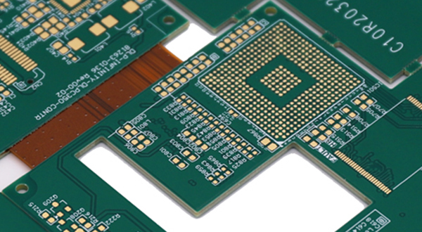
What is Rigid-Flex PCB?

Rigid-Flex PCB is a type of circuit board that combines rigid PCBs and flexible PCBs using layering and hollowing techniques. Rigid-Flex PCBs have the following characteristics:
- High density: Rigid-Flex PCBs can achieve more connections and functions in limited space, reducing the use of plugs and cables and lowering system weight and volume. - High reliability: Rigid-Flex PCBs reduce soldering points and interfaces, improving the stability and durability of the circuit board, and reducing failure rates and maintenance costs. - High flexibility: Rigid-Flex PCBs can bend, fold, or twist according to different design requirements, adapting to various complex shapes and structures.
Applications of Rigid-Flex PCB
Due to these advantages, Rigid-Flex PCB is widely used in the following fields:
- Aerospace: Rigid-Flex PCB can meet the high requirements of aerospace equipment for weight, volume, reliability, and anti-interference, improving equipment performance and safety. - Medical equipment: Rigid-Flex PCB can adapt to the high requirements of medical equipment for flexibility, precision, and biocompatibility, improving equipment efficiency and accuracy. - Smartphones: Rigid-Flex PCB can achieve a compact layout of the internal circuit of smartphones, improving the functionality and aesthetics of the phone.
How to make Rigid-Flex PCB?
The process of making Rigid-Flex PCB mainly includes the following steps:
- Design: According to the product's functionality and shape requirements, design the circuit diagram and layout of the Rigid-Flex PCB, and determine the connection method and turning position between each layer.
- Plate making: Make rigid and flexible boards separately according to the design, and punch holes in the flexible board for subsequent connections.
- Lamination: Stack the rigid and flexible boards according to the design, and cover the flexible board with a semi-cured sheet to protect its surface.
- Hollowing: Process the laminated board by hollowing out the excess parts and forming the required shape.
- Drilling: Drill holes in the hollowed-out board and perform copper plating to form a conductive channel.
- Electroplating: Electroplate the board after drilling to increase the thickness of the conductive layer and form a protective layer.
- Mold making: Make the corresponding printing mold according to the design and place it on the board.
- Printing: Use a printing machine to print the ink onto the board according to the mold and cure it to form the circuit pattern.
- Etching: Remove the excess conductive layer using etching solution and clean it.
- Testing: Use testing instruments to test the electrical performance and appearance quality of the completed board and remove any defective products.
- Cutting: Use a cutting machine to cut the board according to the design and polish the edges.
- Assembly: Weld or plug the cut board with other components and perform functional testing.

