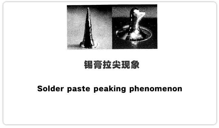
How does solder paste beading occur?

Solder paste beading, commonly known as "solder beading," is a common defect in the PCB assembly process. It is characterized by the formation of pointed extensions or sharp protrusions along the edges of the solder paste after printing. This phenomenon often occurs in fine-pitch pads or between leads, increasing the risk of defects such as short circuits or insufficient solder joints. Solder paste beading can result from various factors, including the printing process, stencil design, solder paste properties, and pad contamination. Below is a detailed analysis of its causes and solutions.
Causes of Solder Paste Beading
Stencil Issues
Improper aperture design: Rough or uneven edges of the stencil apertures can hinder smooth solder paste release.
Mismatched aperture size: Oversized apertures may deposit excessive solder paste, leading to beading, while undersized apertures can cause incomplete release.
Inappropriate stencil thickness: Overly thick stencils increase solder paste deposition, while thinner stencils may lead to incomplete scraping, both contributing to beading issues.
Printing Process Problems
Excessive printing speed: High speeds prevent the solder paste from settling properly, resulting in sharp protrusions at the edges.
Uneven squeegee pressure:Unequal pressure can cause solder paste to overflow or distribute unevenly.
Incorrect squeegee angle:A small angle may leave residual solder paste, while a large angle can hinder proper release.
Solder Paste Properties
High viscosity: Excessive viscosity increases the likelihood of solder paste stretching during printing.
Overactive flux: Highly active flux enhances solder paste fluidity, which may increase the risk of beading.
Aged solder paste: Using solder paste beyond its shelf life can degrade its performance and lead to defects.
PCB Pad Issues
Pad contamination: Oxidation, dirt, or grease on the pad surface can affect solder paste adhesion, leading to uneven distribution.
Warped PCBs: Uneven PCBs may result in inconsistent solder paste thickness, increasing the likelihood of defects.
Impact of Solder Paste Beading
Solder paste beading can cause the following issues:
Short circuit risk: Beads of solder may bridge gaps between pads or leads, causing electrical shorts.
Weak or defective solder joints: Irregular solder joints may compromise mechanical strength or result in poor electrical connectivity.
Increased rework: Defective solder joints require additional repair or rework, reducing production efficiency and yield.
How to Improve Solder Paste Beading
Optimize Stencil Design
Ensure that stencil apertures have smooth, polished edges to reduce defects.
Choose aperture sizes and shapes that match pad dimensions; laser-cut stencils are recommended for precision.
Adjust stencil thickness appropriately, with common values ranging from 0.12mm to 0.15mm, depending on PCB requirements.
Adjust Printing Parameters
Control printing speed and squeegee pressure to prevent excessive paste deposition or uneven distribution.
Optimize the squeegee angle (typically 45° to 60°) to ensure smooth solder paste release.
Regularly inspect printing equipment to ensure stability and consistency.
Select Suitable Solder Paste
Use solder paste with moderate viscosity to avoid excessive or insufficient fluidity.
Ensure that solder paste is within its shelf life and stored correctly to maintain performance.
Select flux activity levels appropriate for specific process requirements to balance adhesion and flow.
Improve PCB Surface Quality Clean pad surfaces to remove oxidation or contaminants; use cleaning agents if necessary.
Choose PCBs with high flatness to reduce the risk of uneven solder paste distribution.
By optimizing stencil design, adjusting printing parameters, selecting appropriate solder paste, and improving PCB surface quality, the occurrence of solder paste beading can be significantly reduced. These measures help enhance soldering quality, improve product reliability, and increase production efficiency.

