
What are the shaping methods of PCB?
In the PCB manufacturing process, the shaping process is a key step that determines the final shape and size of the PCB. Different shaping methods have a direct impact on the production efficiency, cost control, and product quality of the PCB. Let’s take a look at the mainstream PCB shaping methods and their applicable scenarios.
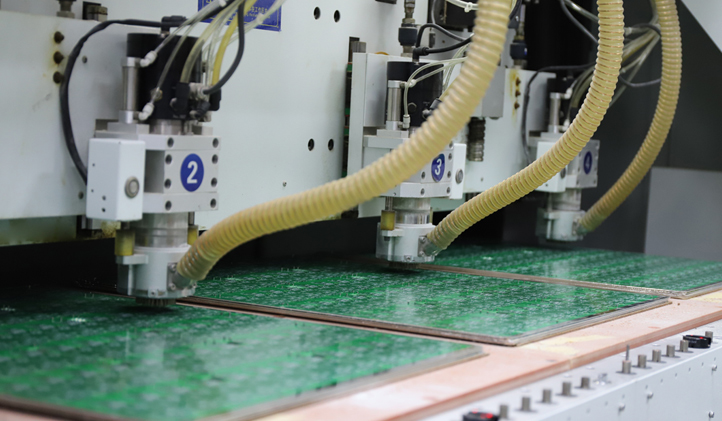
1. CNC Shaping
CNC milling is the most widely used PCB shaping method today. The principle is that a high-speed rotating milling cutter cuts the substrate along a preset path, making it suitable for processing PCBs of any shape. The advantage of CNC is that it offers an accuracy of ±0.1mm and can handle complex contours and internal slots, making it especially suitable for small-batch, multi-variety production. However, due to the single-board processing model, its efficiency is relatively low, and tool wear costs are high. It is commonly used in high-density interconnection (HDI) boards, flexible circuit boards (FPC), and sample-stage verification.
2. V-CUT Shaping
V-CUT (V-shaped cutting) involves pre-cutting V-shaped grooves between the PCB panels, utilizing mechanical stress for rapid board separation. This method has a fast processing speed, with the ability to separate multiple panels at once, making it especially suitable for mass production of rectangular and regular-shaped boards. The cost is only about one-third of that of CNC, but it is limited by the straight-line cutting feature, meaning it cannot handle curved edges. V-CUT also requires attention to the residual burrs, which often need secondary polishing after separation. It is widely used in consumer electronics.
3. Laser Cutting Shaping
Laser cutting uses a high-energy laser beam to vaporize the material, enabling non-contact processing. Its accuracy can reach ±0.05mm, and the cut is smooth with no burrs. This method is particularly suitable for precision processing of ultra-thin boards (below 0.2mm) and brittle materials like ceramic substrates. CO2 lasers are suitable for conventional FR-4 materials, while UV lasers can process flexible materials like polyimide. Although the equipment cost is relatively high (about three times that of CNC), it is irreplaceable in high-end fields such as 5G millimeter-wave antennas and medical micro-devices.
4. Stamping Shaping
Stamping shaping utilizes custom molds for high-speed punching, with the ability to form multiple PCBs in a single punch, achieving a theoretical production capacity of up to 8,000 punches per hour. This process has a very low marginal cost and is suitable for large-scale production of standardized products such as mobile phone motherboards and LED light boards. However, mold development costs are high (ranging from tens of thousands to hundreds of thousands of dollars), and modifications are difficult, making it suitable only for million-piece orders. Recently, the emergence of hydraulic die-cutting technology, which optimizes the mold structure to reduce the minimum hole size to 0.3mm, has expanded the application boundaries of stamping technology.