Skip to content
 Ceramic PCB Manufacturer
The Ultimate Guide to High Performance Circuit
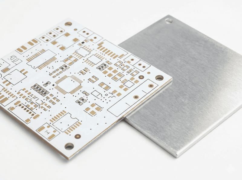
What is a Ceramic PCB?
A ceramic PCB is a specialized circuit board that uses ceramic materials as the base substrate instead of traditional FR4 or other organic materials. These high performance boards are engineered for extreme operating conditions where standard PCBs would fail. I’ve worked with dozens of industrial clients who switched to ceramic PCBs when their applications demanded superior thermal performance and reliability.
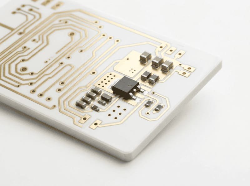
At LZJPCB, our ceramic PCBs feature advanced substrate materials like Aluminum Oxide (Al₂O₃), Aluminum Nitride (AlN), or Silicon Nitride (Si₃N₄), each carefully selected based on your specific application requirements. These materials provide exceptional thermal conductivity, electrical insulation, and mechanical stability that far exceed conventional PCB capabilities. The circuits are typically created using thick film technology, where specialized metallic pastes are screen printed onto the ceramic substrate and then fired at high temperatures to create permanent conductive pathways.
For industrial automation systems operating in harsh environments, ceramic PCBs offer unmatched reliability and performance. When one of my German clients needed control boards for their high temperature industrial processes, ceramic PCBs were the only viable solution, delivering flawless operation where standard boards would quickly degrade.
What are the advantages of Ceramic PCB?
Superior Thermal Management
Ceramic PCBs offer thermal conductivity up to 7-10 times higher than traditional FR4 boards. This exceptional heat dissipation capability prevents hotspots and component failures in high power applications. I recently worked with an industrial automation manufacturer who reduced their control system operating temperature by 35°C simply by switching to AlN ceramic PCBs for their power modules.
The thermal expansion characteristics of ceramic PCBs closely match those of mounted semiconductor devices, significantly reducing thermal stress during temperature cycling. This compatibility is crucial for preventing solder joint failures in applications that experience frequent power cycles or temperature fluctuations. Many of our industrial clients report 3-5x longer service life for power electronics after switching to ceramic based circuit boards.
Extreme Environmental Durability
Ceramic PCBs maintain their electrical and mechanical properties at temperatures ranging from -65°C to over 350°C, far exceeding the capabilities of standard FR4 boards (typically limited to 130-170°C). This wide operating range makes them ideal for industrial equipment exposed to extreme heat or cold. One of our customers uses our ceramic boards in steel mill automation systems where ambient temperatures regularly exceed 200°C.
The chemical inertness of ceramic materials provides exceptional resistance to corrosive substances, humidity, and harsh chemicals that would quickly damage traditional circuit boards. For industrial applications in chemical processing plants or outdoor installations, this translates to significantly longer service life and reduced maintenance costs. The non porous nature of ceramic substrates also prevents moisture absorption that can lead to electrical failures in conventional PCBs.
Enhanced Electrical Performance
Ceramic substrates offer superior electrical insulation properties with dielectric constants ranging from 7-10 and breakdown voltages exceeding 20kV/mm. This enables high voltage applications that would be impossible with standard PCB materials. For industrial clients working with high power motor drives or power conversion systems, ceramic PCBs allow for compact designs without compromising electrical safety.
The low signal loss characteristics of ceramic materials make them ideal for high frequency applications, with minimal signal degradation even at GHz frequencies. This becomes increasingly important as industrial automation systems incorporate wireless technologies and high speed data processing. For precision measurement systems, ceramic PCBs provide stable electrical characteristics across varying environmental conditions, ensuring consistent performance.
What is Ceramic PCB commonly used in?
Power modules and converters benefit tremendously from ceramic PCBs' superior thermal management. The exceptional heat dissipation allows for higher power densities and improved reliability in industrial drive systems and power supplies. I've helped several clients redesign their power conversion modules with ceramic PCBs, achieving 40% size reduction while handling the same power levels.
In high temperature industrial environments like furnace controls, engine management systems, and downhole drilling equipment, ceramic PCBs operate reliably where conventional boards would quickly fail. The thermal stability ensures consistent performance even when ambient temperatures approach 300°C. For a client in the glass manufacturing industry, we developed custom ceramic PCBs that have operated continuously for over five years in 275°C environments, far outlasting their previous solutions.
High power LED modules utilize ceramic PCBs to efficiently transfer heat away from LED components, significantly extending lifespan and maintaining consistent light output. The superior thermal management allows for more compact LED designs with higher brightness levels. Several of our industrial lighting clients have achieved 40-50% longer LED lifespans by switching to ceramic substrates.
Automotive under hood electronics increasingly rely on ceramic PCBs to withstand the extreme temperatures and vibration present in engine compartments. The reliability improvements are substantial, with field failure rates dropping by up to 80% compared to traditional PCB solutions. For electric vehicle manufacturers, ceramic PCBs provide critical thermal management for battery control systems and power conversion modules.
RF and microwave circuits benefit from ceramic substrates' low signal loss and stable dielectric properties, delivering consistent performance across varying environmental conditions. For industrial wireless control systems operating in challenging environments, ceramic PCBs provide the reliability and performance stability required for critical communications.
Aerospace and defense electronics face some of the most demanding operating conditions, making ceramic PCBs an ideal choice for their exceptional reliability and performance. The combination of thermal stability, mechanical strength, and electrical performance ensures mission critical systems operate flawlessly even in extreme conditions. One aerospace client uses our ceramic PCBs in satellite communications equipment where the combination of vacuum conditions and temperature extremes would quickly destroy conventional circuit boards.

Ceramic PCB Design Considerations

Proper thermal design is critical for maximizing ceramic PCB performance. Advanced thermal simulation tools help identify potential hotspots and optimize heat flow patterns before production. Our engineering team uses computational fluid dynamics and finite element analysis to ensure optimal thermal performance for each design. For one industrial power supply manufacturer, our thermal optimization process reduced maximum component temperatures by 28°C while maintaining the same power output.
Strategic via placement and copper pattern design significantly enhance heat spreading across the ceramic substrate. Our design guidelines provide specific recommendations for thermal via patterns based on component power densities and substrate materials. These optimized designs ensure maximum heat transfer without compromising electrical performance or mechanical integrity.
The mismatch between thermal expansion rates of various materials can create mechanical stress during temperature cycling. Proper design techniques minimize this stress to prevent solder joint fatigue or component damage. Our material selection process carefully considers thermal expansion compatibility between substrates, conductors, and mounted components to ensure long term reliability.
For applications experiencing extreme temperature variations, specialized mounting and connection techniques help accommodate thermal expansion differences. Flexible interconnects, compliant die attach materials, and strategic component placement all contribute to improved thermal cycling performance. We've developed specific design rules for different temperature ranges to ensure reliable operation throughout your product's lifetime.
Controlling impedance and minimizing signal losses becomes increasingly important at high frequencies. Our design team provides specific guidelines for transmission line structures on ceramic substrates to ensure optimal electrical performance. For industrial clients working with high speed data acquisition or wireless control systems, these optimized designs deliver superior signal integrity even in noisy industrial environments.
The high dielectric constant of ceramic materials requires different design approaches compared to conventional PCBs. Our engineers adjust trace geometries and spacing to achieve target impedance values while accounting for the unique electrical properties of ceramic substrates. This expertise ensures your ceramic PCB delivers the electrical performance your application demands.
Ceramic PCB manufacturing involves different tolerances and design constraints compared to traditional PCBs. Working within these parameters ensures optimal manufacturability and yield. Our comprehensive design guidelines provide specific recommendations for minimum feature sizes, spacing requirements, and other critical parameters based on your selected manufacturing process and materials.
Early collaboration between design and manufacturing teams helps identify potential issues before they impact production. Our DFM (Design for Manufacturing) review process specifically addresses the unique challenges of ceramic PCB production, ensuring your design is optimized for both performance and manufacturability. This collaborative approach has helped many of our industrial clients achieve first pass manufacturing success even with complex ceramic PCB designs.
Types of Ceramic PCB Materials
Aluminum Oxide (Al₂O₃)

Aluminum Oxide (Alumina) is the most widely used ceramic PCB material, offering an excellent balance of cost and performance. With thermal conductivity of 24-28 W/m·K, it provides significantly better heat dissipation than FR4 while remaining more economical than other ceramic options. For industrial applications with moderate thermal demands, alumina offers an excellent price performance ratio.
Alumina substrates provide excellent electrical insulation properties with dielectric constants around 9.8 and breakdown voltage exceeding 15kV/mm. This makes them ideal for applications requiring high voltage isolation in compact spaces. The material’s chemical stability ensures long term reliability in industrial environments where exposure to moisture and corrosive substances is common.
Aluminum Nitride (AlN)
Aluminum Nitride delivers exceptional thermal performance with conductivity values of 170-230 W/m·K, approaching that of some metals while maintaining excellent electrical insulation. This makes AlN the preferred choice for high power density applications where thermal management is critical. Though more expensive than alumina, AlN can eliminate the need for additional cooling solutions, potentially reducing overall system costs.
The thermal expansion coefficient of AlN closely matches silicon semiconductors, minimizing stress on component connections during temperature cycling. This compatibility is particularly valuable for power modules and other applications subject to frequent thermal cycling. For several of our industrial automation clients, AlN substrates have extended power module lifetime by 300% compared to conventional cooling solutions.

Silicon Nitride (Si₃N₄)

Silicon Nitride offers exceptional mechanical strength and fracture toughness, making it ideal for applications subject to physical stress or vibration. Its combination of mechanical durability and good thermal performance (90-120 W/m·K) makes it well suited for harsh industrial environments. When one of my clients needed circuit boards for high vibration factory equipment, silicon nitride provided the perfect solution, showing no degradation after years of continuous operation.
This material also offers excellent thermal shock resistance, withstanding rapid temperature changes without cracking or delamination. For applications that experience frequent and rapid heating and cooling cycles, silicon nitride provides superior reliability compared to other ceramic options. The material’s resistance to thermal fatigue ensures long term performance in demanding industrial applications.
Low Temperature Co fired Ceramic (LTCC)
LTCC technology enables the creation of complex multilayer ceramic circuits by co firing ceramic and conductive materials at relatively low temperatures (850-900°C). This allows for the integration of resistors, capacitors, and other passive components within the ceramic structure, creating highly integrated modules. For industrial clients needing miniaturized control systems, LTCC technology offers significant size reduction while maintaining excellent thermal performance.
The ability to create three dimensional circuit structures with LTCC technology enables innovative design approaches for space constrained applications. Internal channels can be incorporated for thermal management or fluid sensing applications. Several of our clients in the sensor manufacturing industry use LTCC based designs to create compact, highly integrated sensor modules that outperform conventional approaches.

Ceramic PCB Manufacturing Processes
Thick Film Technology

Thick film processing involves screen printing conductive, resistive, or dielectric pastes onto ceramic substrates, followed by high temperature firing to create permanent circuit elements. This established technology offers excellent reliability and cost effectiveness for most ceramic PCB applications. At LZJPCB, our advanced screen printing equipment achieves line width/spacing down to 100μm, providing excellent circuit density for complex designs.
The thick film process allows for the integration of passive components like resistors and capacitors directly within the circuit structure, reducing component count and improving reliability. For industrial applications, this integration eliminates potential failure points from discrete components and their solder connections. Our precision thick film processing delivers resistor tolerances of ±5%, sufficient for most industrial control applications.
Thin Film Technology

Thin film processing uses vacuum deposition techniques to create extremely precise circuit patterns with feature sizes down to 10μm. This approach offers superior precision and performance for high frequency applications or extremely fine pitch designs. While more expensive than thick film technology, thin film processing delivers unmatched performance for demanding applications.
The enhanced precision of thin film technology enables higher circuit densities and improved electrical performance, particularly for RF/microwave applications. The superior surface finish reduces signal losses and improves reliability of wire bonding and die attach processes. For industrial clients with high precision requirements, our thin film ceramic PCBs provide performance levels unachievable with conventional manufacturing methods.
Direct Bonded Copper (DBC)

DBC technology bonds a thick copper layer (typically 127-500μm) directly to ceramic substrates, creating an extremely robust thermal and electrical interface. The resulting structure offers exceptional current carrying capacity and heat spreading for power electronics applications. Our DBC ceramic PCBs can handle current densities up to 10 times higher than conventional PCBs while maintaining lower operating temperatures.
The direct bonded interface eliminates thermal resistance barriers present in traditional PCBs, maximizing heat transfer from components to the ceramic substrate. This technology is ideal for high power industrial applications like motor drives, power supplies, and induction heating systems. For a client manufacturing industrial motor controllers, our DBC ceramic solution reduced junction temperatures by 45°C while handling 30% more current than their previous design.
Active Metal Brazing (AMB)

AMB technology uses specialized metal alloys to create robust bonds between copper and ceramic substrates, offering superior mechanical strength compared to DBC, particularly for larger substrates. This advanced technique is especially valuable for applications subject to severe thermal cycling or mechanical stress. The improved reliability makes AMB ceramic PCBs ideal for mission critical industrial systems where failure is not an option.
The enhanced mechanical strength of AMB bonds significantly reduces the risk of delamination or cracking during thermal cycling, extending product lifetime in demanding applications. While more expensive than DBC, the improved reliability justifies the cost for critical systems.
Several of our automotive and aerospace clients specify AMB technology exclusively for their most demanding applications due to its exceptional long term reliability.
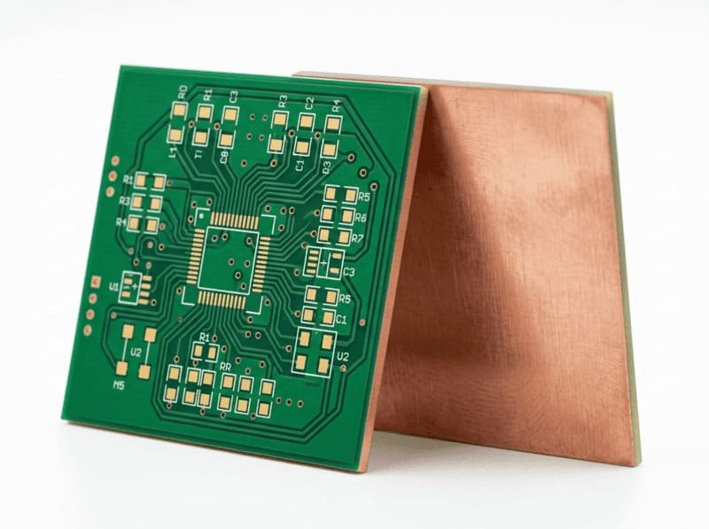
Ceramic PCBs vs. Metal Core PCBs
Thermal Performance Comparison

While metal core PCBs (MCPCBs) offer improved thermal performance over FR4, ceramic PCBs provide significantly superior heat dissipation capabilities. Aluminum MCPCBs typically offer thermal conductivity of 1-3 W/m·K through their dielectric layer, while ceramic PCBs range from 24-230 W/m·K depending on the material. This dramatic difference becomes critical in high power density applications where every degree of temperature reduction matters.
The thermal advantage of ceramic PCBs becomes even more pronounced at elevated temperatures, where their thermal properties remain stable while MCPCBs may degrade. For industrial applications operating near their thermal limits, this stability ensures consistent performance and reliability. I’ve seen numerous cases where clients attempted to use MCPCBs for high temperature applications, only to switch to ceramic substrates after experiencing premature failures.
Electrical Insulation Properties

Ceramic substrates provide superior electrical isolation with breakdown voltages exceeding 15kV/mm, compared to 4-8kV/mm for typical MCPCB dielectric layers. This enhanced insulation capability enables higher voltage designs in more compact spaces. For industrial power systems operating at elevated voltages, ceramic PCBs allow for smaller clearances while maintaining safety margins.
The excellent dielectric properties of ceramics remain stable across a wide temperature range, unlike organic dielectrics used in MCPCBs which may degrade at elevated temperatures. This stability ensures consistent electrical performance even in extreme operating conditions. Many of our industrial clients specify ceramic PCBs specifically for their superior insulation properties in safety critical applications.
Long Term Reliability Considerations

Ceramic PCBs maintain their properties virtually indefinitely, showing minimal degradation even after years of operation at elevated temperatures. In contrast, the organic dielectric layers in MCPCBs can gradually deteriorate when exposed to high temperatures or thermal cycling. For industrial equipment designed for decades of service, this long term stability provides significant value despite the higher initial cost.
The chemical inertness of ceramic materials provides exceptional resistance to environmental factors that may degrade MCPCBs over time. Humidity, corrosive atmospheres, and UV exposure have minimal impact on ceramic substrates, making them ideal for harsh industrial environments. When total lifecycle cost and reliability are primary concerns, ceramic PCBs often prove more economical despite their higher initial price.
Cost and Manufacturability Comparison

Metal core PCBs generally offer lower initial costs and can utilize much of the same manufacturing equipment as standard FR4 boards. This makes MCPCBs an attractive option for less demanding thermal applications where cost is a primary concern. For moderate thermal requirements with budget constraints, our engineering team often recommends optimized MCPCB designs as a cost effective solution.
Ceramic PCBs require specialized manufacturing processes and equipment, contributing to their higher cost. However, this premium is often justified by their superior performance and reliability in demanding applications. For many industrial clients, the extended service life and improved performance of ceramic PCBs deliver better long term value despite the higher initial investment.
LZJPCB Ceramic PCB Manufacturing Capabilities
| Features | Capabilities |
|---|---|
| Substrate Materials | Aluminum Oxide (Al₂O₃), Aluminum Nitride (AlN), Silicon Nitride (Si₃N₄), LTCC |
| Substrate Thickness | 0.25mm to 2.5mm standard, custom thicknesses available |
| Maximum Board Size | Up to 200mm × 250mm (larger sizes available through tiling techniques) |
| Minimum Line Width | 100μm (thick film), 10μm (thin film) |
| Minimum Line Spacing | 100μm (thick film), 10μm (thin film) |
| Surface Finish Options | Silver, Gold, Nickel-Gold, Platinum-Gold, Palladium-Silver |
| Via Technology | Laser drilled vias, through-hole vias, thermally conductive vias |
| Metallization Thickness | 5μm to 500μm depending on process and requirements |
| Layer Count | Single layer to 30+ layers (LTCC technology) |
| Integrated Components | Resistors, capacitors, inductors (thick film and LTCC) |
| Manufacturing Processes | Thick film, thin film, DBC (Direct Bonded Copper), AMB (Active Metal Brazing) |
| Typical Lead Times | Prototype: 1-2 weeks, Production: 2-4 weeks |
| Special Features | 3D structures (LTCC), embedded cooling channels, hermetic packaging capabilities |
| Testing | 100% electrical testing, thermal imaging, X-ray inspection, mechanical stress test |
| Quality Standards | ISO 9001:2015, IPC standards, MIL standards compliance |
Why Choose LZJPCB for Ceramic PCB Manufacturing?
Technical Expertise and Design Support
Our engineering team specializes in ceramic PCB design and manufacturing, with decades of combined experience in high performance circuit applications. We don't just manufacture your design, we help optimize it for maximum performance and reliability. For every ceramic PCB project, we provide comprehensive design reviews focused on thermal management, electrical performance, and manufacturing optimization.
I personally work with many of our industrial clients during the early design phases, providing material recommendations and design guidelines specific to their application requirements. Our collaborative approach ensures your ceramic PCB design leverages our manufacturing expertise for optimal results. This partnership has helped countless clients avoid costly design iterations and achieve superior performance from their first prototype.
Advanced Manufacturing Capabilities
LZJPCB has invested in specialized equipment and processes specifically for ceramic PCB manufacturing. Our dedicated ceramic production lines maintain strict quality controls throughout the manufacturing process. Our facilities include advanced screen printing systems capable of fine line definition, precisely controlled firing ovens, and specialized test equipment for ceramic substrates.
Our manufacturing capabilities span the full range of ceramic PCB technologies, from standard thick film processes to advanced thin film, DBC, and LTCC technologies. This versatility allows us to recommend the most appropriate manufacturing approach based on your specific technical requirements and budget constraints. For industrial clients with unique requirements, we can develop custom manufacturing processes tailored to your specific application.
Proven Success with Industrial Clients
Our portfolio includes successful ceramic PCB projects for leading industrial automation companies worldwide. We've helped clients solve critical thermal management challenges, improve product reliability in harsh environments, and reduce the size of power electronics systems. Our manufacturing processes meet the stringent requirements of international standards for both industrial and military applications.
Working with industrial clients across Europe, Asia, and North America has given us deep insight into the specific requirements of industrial control systems. We understand the importance of long term reliability, consistent performance across varying environmental conditions, and compatibility with existing manufacturing processes. Our ceramic PCB solutions are specifically engineered to address these critical industrial requirements.
Ceramic PCB FAQ
What are the minimum feature sizes possible on ceramic PCBs?
Feature sizes vary significantly depending on the manufacturing process:
– Thick film technology typically achieves line width/spacing of 100-150μm (4-6 mil)
– Thin film technology can reach 10-25μm (0.4-1 mil) for extremely precise applications
– DBC processes typically achieve 200-300μm (8-12 mil) minimum features
For most industrial applications, our standard thick film processes provide sufficient resolution while maintaining excellent cost effectiveness. When your application demands finer features, our thin film capabilities deliver exceptional precision. During our design review process, we’ll recommend the most appropriate manufacturing approach based on your specific requirements.
How do ceramic PCBs handle thermal cycling?
Ceramic PCBs demonstrate excellent thermal cycling resilience, particularly when properly designed to account for thermal expansion differences. Material selection plays a critical role – Aluminum Nitride (AlN) has a coefficient of thermal expansion closely matching silicon semiconductors, minimizing stress during temperature cycling.
For applications experiencing extreme temperature variations, we implement specific design techniques:
– Optimized pad geometries to reduce stress concentration
– Specialized metallization systems with improved adhesion
– Strategic component placement to accommodate expansion differences
– Appropriate die attach materials to buffer thermal stress
One of our industrial clients uses our ceramic PCBs in equipment cycling between -40°C and +200°C daily. After five years of operation, they report zero failures – a testament to proper design and material selection for thermal cycling applications.
What surface finishes are available for ceramic PCBs?
We offer several metallization options for ceramic PCBs, each with specific advantages:
– Silver: Excellent conductivity and solderability, cost effective for many applications
– Gold: Superior oxidation resistance and wire bondability, ideal for harsh environments
– Nickel Gold: Combines nickel’s solderability with gold’s environmental protection
– Platinum Gold: Exceptional high temperature stability for extreme applications
– Palladium Silver: Good solderability with improved migration resistance
For industrial applications, we often recommend nickel gold finishes due to their excellent combination of solderability, environmental resistance, and long shelf life. Our engineering team can recommend the optimal surface finish based on your specific assembly process, operating environment, and reliability requirements.
Can ceramic PCBs be repaired if damaged?
Unlike traditional PCBs, ceramic circuits have limited repair options once fired. Minor repairs are possible through techniques like:
– Laser trimming for resistor value adjustment
– Wire bonding to bypass damaged traces
– Specialized conductive adhesives for localized repairs
For critical applications, we recommend a design approach that incorporates redundancy in critical circuits and allows for module replacement rather than board level repair. During the design phase, we can help identify potential vulnerability points and implement appropriate redundancy measures.
For industrial clients with field serviceability requirements, we often design ceramic PCB systems with modular approaches, allowing replacement of smaller subassemblies rather than entire systems. This strategy balances the inherent repair limitations of ceramic technology with practical field maintenance needs.
How do I determine if my application requires ceramic PCBs?
Ceramic PCBs are typically justified when your application involves one or more of these factors:
– Operating temperatures exceeding 150°C
– High power density requiring superior thermal management
– Exposure to harsh chemical environments
– Critical reliability requirements in extreme conditions
– High frequency operation requiring stable dielectric properties
Our engineering team provides free application assessments to determine if ceramic technology is appropriate for your specific needs. We often find that hybrid approaches – using ceramic PCBs only for critical high stress portions of the system – provide the optimal balance of performance and cost.
For industrial automation applications, we evaluate factors like ambient operating temperature, power dissipation requirements, expected service life, and environmental exposure to recommend the most appropriate substrate technology. This consultative approach ensures you get the performance you need without unnecessary cost.
What are the cost factors for ceramic PCBs compared to standard PCBs?
Ceramic PCBs typically cost 3-10 times more than standard FR4 boards, depending on several factors:
– Substrate material choice (Alumina is most economical, AlN and Si₃N₄ more expensive)
– Manufacturing process complexity (thick film vs. thin film vs. DBC)
– Circuit complexity and feature sizes
– Production volume (economies of scale apply)
However, this cost comparison must consider the total system cost, including:
– Elimination of separate heat sinks or cooling systems
– Reduced assembly complexity
– Extended service life and reliability improvements
– Enablement of designs not possible with standard PCBs
For many industrial applications, the performance advantages and long term reliability benefits justify the higher initial investment. Our engineering team can help perform cost benefit analyses for your specific application to determine if ceramic technology provides the best overall value.
Unlock More Possibilities with LZJPCB Solutions
From standard PCBs to advanced ceramic technologies, our manufacturing services deliver exceptional quality across diverse applications and industries. Contact us today to discover how our ceramic PCB solutions can elevate your next project to new levels of performance and reliability.
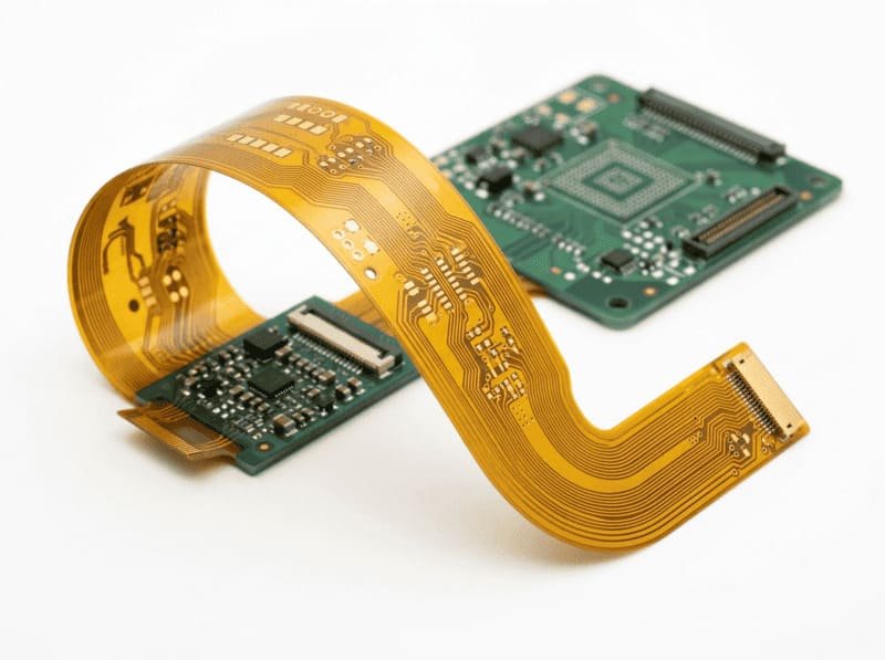
Flex PCB
- Layer count: 1-32 layers
- Turn time: from 24 hours
- Thickness: 0.4mm-4.0mm
- Copper: 1-15oz
- Min trace/spacing: 3/3 mil
HDI PCB
- 4-20 layer HDI designs
- Advanced buried and blind via technology
- 10 day production timeline
- Ideal for complex, space constrained applications
Rogers PCB
- 5 day production timeline
- Premium RO4003C and RO4350B materials
- Specialized for RF and high frequency applications
- Exceptional signal integrity performance
Aluminum PCB
- 1-2 layer designs
- 24 hour rapid production available
- Thickness options: 0.8mm-3.2mm
- Copper weights: 0.5-4oz
- Precision trace/spacing down to 3/3 mil
- Enhanced thermal dissipation
Copper Core PCB
- 1 - 2 layer configurations
- 1.0-2.0mm thickness options
- 1-2oz copper weights
- Superior thermal management properties
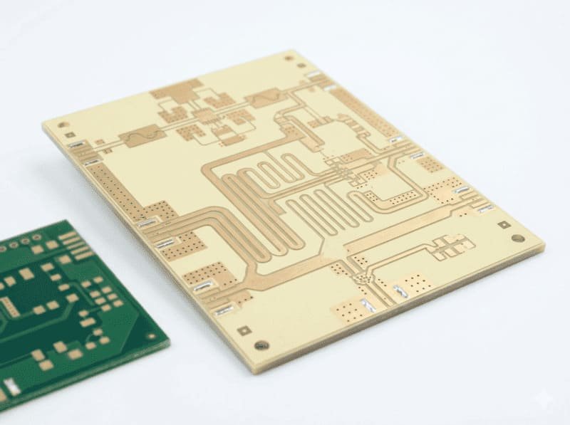
Ceramic PCB
- Layer count: 1-2 layers
- Turn time: from 24 hours
- Thickness: 0.8mm-3.2mm
- Copper: 0.5-4oz
- Min trace/spacing: 3/3 mil
Get Your Turnkey PCB Manufacturing Quote Within 12 Hours
Our experienced engineering team will analyze your requirements and provide a detailed production plan with transparent pricing.