Skip to content
 Flex PCB Manufacturer
The Ultimate Guide to Flexible Circuit Boards
What is a Flex PCB?
Flex PCBs (Flexible Printed Circuit Boards) are electronic circuit boards built on flexible polymer substrates that can bend, fold, and twist while maintaining electrical functionality. Unlike traditional rigid FR4 boards, flex PCBs use thin, pliable materials typically polyimide (Kapton®) or polyester (PET) that allow the circuit to conform to three dimensional shapes and dynamic applications.
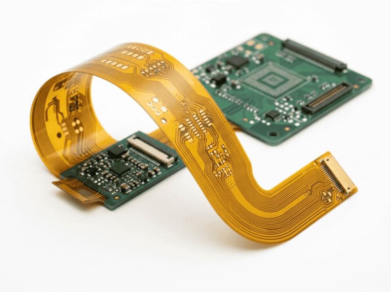
At LZJPCB, we manufacture flex PCBs with precision copper traces as thin as 2 mil (0.05mm) on substrates as thin as 0.1mm. This creates incredibly lightweight and space efficient circuits that can be deployed in applications where rigid boards simply can’t function. Our flex circuits range from simple single sided designs to complex multi layer constructions, supporting both static flex (bent once during installation) and dynamic flex (continuous movement during operation) requirements.
The ability to eliminate bulky wire harnesses and connectors makes flex PCBs indispensable for modern electronics that demand reliability in compact spaces. For industrial automation equipment like Michael’s control systems, flex PCBs deliver the perfect combination of space savings, weight reduction, and reliability improvement.
What are the advantages of Flex PCB?
Design Freedom and Space Optimization
Flex PCBs can fold around corners, fit into tight spaces, and conform to complex three dimensional shapes—impossible feats for rigid boards. This design flexibility reduces overall system size by up to 60% compared to traditional rigid board assemblies with connectors. In one recent industrial automation project I worked on, replacing a bulky wire harness with a custom flex circuit reduced the control cabinet volume by nearly 40% while improving reliability.
The ability to create custom 3D interconnection paths means your electronic designs aren't limited to flat surfaces. Flex circuits can route through narrow openings, around obstacles, and connect multiple planes without additional connectors. This design freedom is particularly valuable for industrial equipment with space constraints or complex internal geometries.
Weight Reduction
Flex PCBs typically weigh 75% less than comparable rigid board assemblies. A standard flex circuit using 1oz copper on 2mil polyimide weighs approximately 2.8g per square inch, compared to 12g for a typical rigid FR4 board with connectors. This dramatic weight reduction becomes significant when multiplied across numerous boards in complex industrial systems.
The weight savings directly translate to lower shipping costs, reduced mechanical stress on mounting points, and less material consumption all contributing to both economic and environmental benefits. For industrial automation equipment that might be mounted on moving parts or robotic systems, this weight reduction can improve system performance by reducing inertial loads.
Reliable Dynamic Performance
Unlike rigid boards connected by wires or cables, flex PCBs maintain consistent electrical performance during movement. Our polyimide based circuits can withstand over 1 million flex cycles without failure when properly designed with dynamic flex zones. This exceptional durability eliminates common failure points like solder joints and connector pins that plague traditional assemblies.
I recently helped a German industrial automation client redesign their robotic control system using flex PCBs, eliminating cable failures that had caused costly downtime. After implementing our flex circuit solution, they reported zero connection failures over 18 months of continuous operation a dramatic improvement over their previous 3 month average failure cycle with conventional wiring.
What is Flex PCB commonly used in?
Industrial control systems benefit tremendously from flex PCBs' ability to fit into tight spaces while providing reliable connections between components. In modern factory automation equipment, flex circuits connect multiple sensor inputs and control outputs while navigating through compact machine structures.
Our flex PCBs have been deployed in industrial controllers where their space saving design allowed for significant miniaturization without compromising functionality. One client reduced their control unit footprint by 35% by replacing rigid boards and connectors with a custom rigid-flex design, enabling installation in locations previously considered too small for intelligent control systems.
The reliability improvements are equally significant. By eliminating connector failures a leading cause of industrial equipment downtime flex PCB based control systems deliver higher uptime and lower maintenance costs, critical advantages for production environments where every minute of downtime represents significant financial loss.
Motion control applications present the perfect use case for dynamic flex PCBs, which must reliably transmit signals while undergoing repeated movement cycles. Our specialized flex circuits designed for continuous motion can withstand millions of flex cycles without failure when properly designed with graduated bend radii and appropriate copper pattern optimization.
For industrial robotics, CNC machines, and other motion control systems, flex PCBs eliminate the cable management challenges associated with moving components. By replacing bulky cable chains with thin, lightweight flex circuits, equipment designers can achieve faster movement speeds, lower power consumption, and reduced mechanical complexity.
I recently worked with a European industrial automation manufacturer to redesign their robotic arm control system using custom flex circuits. The new design eliminated cable failures that had plagued their previous design while reducing system weight by 28%, allowing for faster arm movement speeds and improved positioning accuracy.
Modern industrial sensors and instrumentation increasingly rely on flex PCBs to minimize size while maximizing reliability. From temperature sensors that must conform to curved surfaces to vibration monitors installed in tight machinery spaces, flex circuits enable sensing capabilities in locations where rigid boards simply won't fit.
Our flex PCB designs for sensing applications incorporate specialized features like selective stiffeners that provide rigid mounting areas for sensitive components while maintaining flexibility where needed. For applications requiring both high component density and installation flexibility, rigid-flex designs offer the perfect balance.
The thermal management advantages of thin flex circuits also benefit sensor applications. With thickness as low as 0.1mm, flex PCBs dissipate heat more efficiently than thicker rigid boards, helping maintain measurement accuracy in temperature sensitive instrumentation.

Design Considerations for Flex PCB

Material selection critically impacts flex PCB performance, with substrate choices determining flexibility, temperature resistance, and long term reliability. Polyimide (like DuPont's Kapton®) remains the gold standard for industrial applications due to its outstanding temperature range (-200°C to +400°C), chemical resistance, and mechanical durability.
For applications requiring lower cost and moderate performance, PET (polyethylene terephthalate) offers good flexibility and electrical properties at reduced cost, though with a more limited temperature range (-40°C to +105°C). Advanced applications might utilize LCP (Liquid Crystal Polymer) for exceptional high frequency performance or PEEK (Polyetheretherketone) for extreme chemical resistance.
At LZJPCB, we primarily work with polyimide based materials for industrial applications, as they deliver the reliability and temperature performance industrial environments demand. For cost sensitive projects with less demanding requirements, we offer PET based alternatives that maintain good performance while reducing overall project costs.
Proper bend radius design directly determines flex circuit lifespan. For static applications (bent once during installation), we typically design flex circuits with minimum bend radii of 6-10 times the circuit thickness. Dynamic applications (continuous flexing) require more conservative designs with bend radii 10-15 times the circuit thickness and specialized copper pattern optimization.
Our design team implements advanced techniques like graduated bend radii, crosshatched copper patterns in flex zones, and specialized stacked layer arrangements to optimize performance in bend areas. These approaches distribute stress more evenly across the circuit, dramatically extending operational life in dynamic applications.
For a recent industrial automation project, we implemented a dual radius design where the initial installation bend used a tighter radius, but the section subject to repeated movement incorporated a larger radius with specialized copper pattern optimization. This hybrid approach maximized space efficiency while ensuring the 10+ year operational life the application required.
Component placement on flex circuits requires careful consideration of mechanical stresses, thermal effects, and manufacturing requirements. We recommend locating components away from bend areas whenever possible, using rigid or stiffened sections for component mounting to prevent stress concentration at solder joints.
When components must be placed near bend areas, our design team implements specialized techniques like "strain relief" patterns that gradually transition from rigid component mounting areas to flexible sections. For components that generate significant heat, we create thermal management structures like copper pours or localized stiffeners that help dissipate heat while maintaining overall flexibility.
Surface mount components typically perform better than through hole on flex circuits, as they introduce less mechanical stress into the substrate. For applications requiring through hole components, we implement reinforced plating and specialized pad designs to ensure long term reliability despite the additional stress.
Types of Flex PCBs
Single Sided Flex PCBs

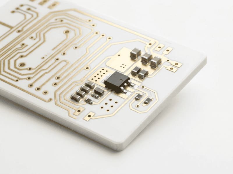
Single sided flex PCBs feature conductive copper traces on only one side of the flexible substrate, with a coverlay (flexible solder mask) protecting the circuits. This simplest flex configuration offers maximum flexibility and lowest cost, making it ideal for basic interconnections and simple control circuits.
Our manufacturing process for single sided flex starts with precision etching of copper traces as narrow as 3mil (0.076mm) on polyimide substrates as thin as 12.5µm (0.5mil). The exposed copper is typically protected with either a coverlay or a flexible solder mask, with selective gold plating available for connection areas requiring exceptional reliability or frequent mating cycles.
Single sided flex PCBs are perfect for applications requiring simple connections in tight spaces, like sensor interfaces or LED control circuits. Their extreme flexibility allows them to be folded into compact geometries with bend radii as small as 3mm for polyimide based circuits.
Double Sided Flex PCBs
Double sided flex PCBs carry conductive traces on both sides of the substrate, connected through plated through holes or vias. This configuration significantly increases circuit density while maintaining good flexibility, offering an excellent balance between design complexity and bending performance.
Manufacturing double sided flex requires precise alignment between layers and specialized plating techniques to ensure reliable connections through the flexible substrate. Our advanced registration systems maintain layer to layer alignment within ±0.05mm, ensuring consistent electrical performance even in densely populated designs.
For industrial control systems requiring moderate circuit complexity with some flexibility, double sided flex offers an ideal balance. These circuits can incorporate ground planes for improved signal integrity while still maintaining enough flexibility for installation in complex equipment geometries.

Multi Layer Flex PCBs

Multi layer flex PCBs stack multiple conductive layers with insulating materials between them, creating complex circuits that remain somewhat flexible. These sophisticated structures can incorporate dedicated power and ground planes, controlled impedance traces, and high component density while maintaining some bending capability.
Our manufacturing capabilities include flex circuits with up to 8 conductive layers, using advanced lamination techniques that maintain flexibility in specific designed bend areas while providing the electrical performance of conventional multi layer boards. These sophisticated structures enable complex circuits in applications where rigid boards won’t fit or where weight must be minimized.
Multi layer flex PCBs excel in high density applications requiring sophisticated circuit functionality in non planar configurations. They’re particularly valuable in industrial equipment where control circuits must fit into complex three dimensional spaces while maintaining high signal integrity.
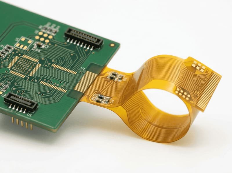
Rigid-Flex PCBs
Rigid flex PCBs combine flexible circuit areas with rigid board sections in a single integrated structure. This hybrid approach provides the perfect balance between the mechanical support and component mounting capabilities of rigid boards with the space saving flexibility of flex circuits.
Our rigid flex manufacturing integrates FR4 or other rigid materials in specific areas designed for component mounting, while maintaining flexible sections for dynamic bending or installation routing. The transition between rigid and flexible sections is carefully engineered to ensure long term reliability, with specialized techniques to manage stress concentrations at these critical interfaces.
Rigid flex PCBs offer the ultimate solution for complex electronic systems where components must be mounted securely but interconnections need to navigate three dimensional paths. They eliminate connectors between boards, dramatically improving reliability while reducing assembly costs and overall system size.
Manufacturing Process for Flex PCBs
Material Preparation

The flex PCB manufacturing process begins with precision preparation of the base materials. We typically start with copper clad polyimide or PET laminates, available in thicknesses ranging from 12.5µm to 125µm (0.5mil to 5mil). The copper foil, typically ranging from 1/3oz (12µm) to 2oz (70µm), is either roll bonded to the substrate during manufacture or applied using specialized adhesives.
For multi layer designs, we prepare multiple sheets of these materials along with bondply (adhesive sheets) that will join the layers during lamination. Each material is inspected for defects and acclimatized in controlled humidity environments to ensure dimensional stability during processing.
Unlike rigid board manufacturing, flex PCB production demands exceptional care in material handling to prevent damage to the thin, flexible substrates. Our specialized material preparation area maintains strict environmental controls and uses automated handling equipment to minimize potential damage during this critical first step.
Imaging and Etching
Creating the conductive circuit pattern on flex PCBs requires precision imaging and etching processes. We apply photosensitive resist to the copper surfaces, then expose them through high resolution photomasks that define the circuit pattern with accuracy down to 2mil (0.05mm) line widths and spacing.
After developing the photoresist, our controlled etching process removes unwanted copper while protecting the circuit traces. This process requires tighter controls than rigid board manufacturing due to the thinner materials and finer features typical of flex designs. Our specialized equipment maintains etching parameters within ±5% tolerance, ensuring consistent trace dimensions critical for impedance control and flexibility performance.
For multi layer designs, each layer undergoes this process individually before lamination. The imaging systems utilize precision registration features that enable layer to layer alignment accuracy of ±0.05mm in the completed circuit.

Coverlay Application

Rather than the hard solder mask used on rigid boards, flex PCBs typically use coverlay a flexible protective layer (usually polyimide with adhesive) that covers and protects the copper traces while leaving connection areas exposed. This coverlay provides both electrical insulation and mechanical protection for the delicate circuits.
Our coverlay application process involves precision cutting of openings using either laser or mechanical methods, followed by vacuum lamination that ensures complete adhesion without trapped air bubbles that could compromise flexibility or reliability. The coverlay thickness typically ranges from 12.5µm to 50µm (0.5mil to 2mil), with adhesive layers adding another 12.5µm to 25µm (0.5mil to 1mil) of thickness.
For applications requiring exceptional flexibility, we offer selective coverlay application that leaves bend areas with minimal covering, reducing overall thickness in these critical zones while maintaining protection over circuit features requiring it.
Final Processing and Testing
The final manufacturing stages include drilling or punching of mounting holes, application of surface finishes (typically ENIG, immersion tin, or OSP for flex circuits), singulation (separating individual circuits from production panels), and comprehensive electrical testing.
Our automated optical inspection (AOI) systems verify proper circuit pattern formation, coverlay alignment, and feature positioning. Every flex PCB undergoes electrical continuity and isolation testing, with impedance testing performed on designs with controlled impedance requirements.
For flex circuits designed for dynamic applications, we perform flex testing on samples from each production lot, subjecting them to accelerated cycling that verifies performance to specification. This ensures that the manufactured circuits will withstand their intended operating conditions throughout their designed lifetime.

What is the difference between flex and rigid PCB?
Material Composition

Flex PCBs use thin, pliable substrates—primarily polyimide (0.0005″ to 0.005″ thick) that allow the circuit to bend and flex during use. This flexible substrate forms the foundation of the circuit’s mechanical properties, with specialized adhesives bonding copper layers to the base material. The entire structure remains thin and pliable, with typical overall thicknesses between 0.1mm and 0.3mm for single or double sided designs.
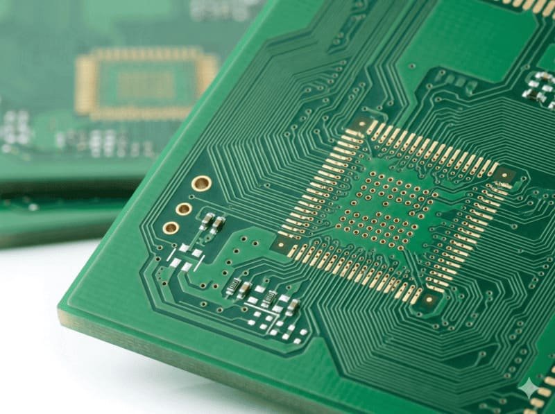
In contrast, rigid PCBs use FR4 glass epoxy substrates that provide structural rigidity and dimensional stability. These substrates typically range from 0.4mm to 3.2mm thick and create a solid, inflexible foundation for mounting components. The woven fiberglass reinforcement in FR4 delivers excellent mechanical strength but makes bending impossible without breaking the board.
During a recent factory tour with an industrial client, I demonstrated this fundamental difference by flexing a polyimide circuit to a 5mm bend radius while explaining how an FR4 board of the same thickness would immediately fracture under similar deformation. This visual demonstration helped the client understand why flex technology was essential for their space constrained application.
Design Philosophy

Designing flex PCBs requires a fundamentally different approach that considers mechanical movement as a primary design parameter. Flex designs must carefully plan bend areas, using curved traces (rather than 90° angles) to distribute stress, placing components away from flex zones, and implementing gradual transitions between different board sections. The entire design process treats the circuit as both an electrical and a mechanical system.
Rigid PCB design, while still requiring attention to mechanical factors, focuses primarily on electrical performance, component placement density, and thermal management. Designers can place components and route traces anywhere on the board’s surface without worrying about bend stresses or movement related failures. This simplifies the design process but limits the board to flat, static applications.
I recently helped a German automation manufacturer transition from rigid to flex technology for a robotic control system. The learning curve involved understanding this new design philosophy—treating the circuit as a dynamic mechanical system rather than just an electrical platform. Once their engineering team embraced this perspective, they were able to leverage flex technology’s full potential to create a dramatically more reliable and compact solution.
Manufacturing Processes

Flex PCB manufacturing involves specialized processes designed for handling thin, pliable materials. Rather than the hard solder mask used on rigid boards, flex circuits use polyimide coverlay applied through precision vacuum lamination processes. Specialized handling equipment prevents damage to delicate materials during production, and unique registration systems maintain layer alignment despite the substrate’s inherent dimensional instability.
Rigid PCB manufacturing uses more robust processes optimized for FR4 and similar materials, with standard handling equipment, screen printed solder mask application, and established plating processes. The manufacturing line can process boards more rapidly and with less specialized equipment, contributing to rigid PCBs’ lower cost structure.
These manufacturing differences directly impact both cost and lead time. Our flex PCB production typically requires 2-3 additional days compared to equivalent rigid designs, with prices roughly 2-3 times higher due to specialized materials and processes. However, for applications requiring three dimensional interconnection, the system level benefits of flex technology far outweigh these additional costs.
Application Suitability
Flex PCBs excel in applications requiring:
Movement during operation (dynamic flex)
Bending during installation (static flex)
Extremely thin profile (0.1mm-0.3mm)
Lightweight construction (75% weight reduction vs. rigid)
Three dimensional interconnection paths
High reliability in vibration environments
Rigid PCBs are superior for applications requiring:
Maximum component density
Lowest possible cost
Thermal dissipation (especially with metal core options)
Structural support for heavy components
Simplest manufacturing process
Standard design methodologies
The choice between these technologies should be driven by application requirements rather than familiarity or initial cost. For example, in a recent industrial automation project, we replaced five interconnected rigid boards with a single rigid-flex assembly, reducing assembly time by 60% while eliminating multiple failure prone connectors. Despite the higher per board cost, the system level savings and reliability improvements delivered substantial value to the client.
Performance Characteristics
- Flex PCBs offer unique performance advantages including:
Superior vibration resistance (no rigid solder joints to crack)
Excellent high cycle flex durability (>1 million cycles when properly designed)
Better thermal cycling performance (accommodates expansion/contraction)
Reduced electromagnetic interference (EMI) in specific designs
Space and weight savings of 60-75% compared to rigid equivalentsRigid PCBs provide different performance benefits:
Better heat dissipation for high power components
Superior support for large or heavy components
Lower cost for equivalent circuit complexity
Simpler assembly processes with standard equipment
More familiar design rules and manufacturing processesFor industrial automation applications specifically, the choice often depends on installation environment and mechanical constraints. Control systems requiring installation in tight spaces with complex geometries benefit tremendously from flex technology, while equipment with adequate space and minimal vibration may be better served by conventional rigid boards.
LZJPCB Flex PCB Manufacturing Capabilities
| Features | Capabilities |
|---|---|
| Circuit Types | Single sided, Double sided, Multi layer (up to 8 layers), Rigid-Flex |
| Material Options | Polyimide (Kapton®), PET, LCP, Advanced materials available on request |
| Minimum Line Width/Spacing | 3/3 mil (0.076mm) standard, down to 2/2 mil (0.051mm) for advanced designs |
| Board Thickness | 0.1mm to 3.2mm (varies by construction) |
| Surface Finish Options | ENIG, Immersion Tin, OSP, Selective Hard Gold |
| Copper Weight | 1/3 oz to 2 oz (12µm to 70µm) |
| Minimum Hole Size | 0.15mm mechanical drilling, 0.1mm laser drilling |
| Dynamic Flex Capability | Designs optimized for >1 million flex cycles in controlled bend areas |
| Coverlay Options | Polyimide, Photoimageable coverlay, Flexible solder mask |
| Stiffener Options | FR4, Polyimide, Stainless Steel, Aluminum |
| Testing | 100% electrical testing, AOI inspection, Dynamic flex testing, Custom testing available |
| Typical Lead Times | Prototype: 3-5 business days Standard Production: 7-10 business days Volume Production: 2-3 weeks |
Why Choose LZJPCB for Flex PCB?
Engineering Partnership
Our approach goes beyond simple manufacturing we partner with your engineering team to optimize flex PCB designs for both performance and manufacturability. With dedicated flex circuit experts who understand both electrical and mechanical aspects of these specialized boards, we help identify potential issues before production and suggest improvements that enhance reliability while reducing costs.
I personally work closely with clients like industrial automation manufacturers to understand their unique requirements, often suggesting innovative approaches that leverage the full potential of flex technology. This collaborative engineering approach has helped numerous clients overcome complex design challenges while meeting strict performance requirements.
In one recent project, our engineering team redesigned a complex industrial sensor package to use a rigid-flex approach rather than multiple interconnected boards. The resulting design reduced assembly time by 65%, eliminated five potential failure points, and allowed the system to fit in a housing 40% smaller than the original concept.
Quality Assurance
Our flex PCB manufacturing facilities implement rigorous quality control procedures specifically designed for these specialized circuits. From incoming material inspection through final electrical testing, each step includes verification processes that ensure your flex circuits will perform as designed in your industrial automation equipment.
Our quality management system maintains ISO 9001:2015 and ISO 13485:2016 certifications, with manufacturing processes that meet or exceed IPC-6013 standards for flexible circuits. Each production lot undergoes comprehensive testing including automated optical inspection, electrical continuity/isolation testing, and dimensional verification.
For critical industrial applications, we offer extended reliability testing including dynamic flex testing, environmental stress screening, and cross sectional analysis. These additional verification steps provide confidence that your flex circuits will maintain performance throughout their intended operational lifetime, even in demanding industrial environments.
Global Manufacturing Footprint
With manufacturing facilities in both China and Indonesia, LZJPCB offers exceptional flexibility to meet diverse project requirements. Our China facility specializes in high complexity, advanced technology flex circuits, while our Indonesia location provides cost competitive solutions for higher volume production.
This distributed manufacturing capability ensures business continuity through geographic diversification while offering options that balance technical requirements, cost targets, and regional preferences. For European industrial clients like Michael's company, our global footprint provides supply chain security through multiple sourcing options while still delivering consistent quality.
Both facilities maintain identical quality standards and use consistent processes, ensuring that your flex PCB designs can be manufactured at either location with equivalent results. This manufacturing flexibility has proven particularly valuable for clients navigating recent global supply chain challenges.
Flex PCB FAQs
What are the typical lead times for flex PCB production?
Our typical lead times for flex PCB production are:
– Prototype quantities (1-10 pieces): 3-5 business days
– Standard production (10-500 pieces): 7-10 business days
– Volume production (500+ pieces): 2-3 weeks
For urgent projects, we offer expedited services that can reduce these timelines by 30-50%, depending on design complexity and current production capacity. Our dual manufacturing locations also provide additional flexibility for meeting critical deadlines.
Industrial clients with scheduled production requirements can benefit from our reserved capacity program, which guarantees manufacturing slots for regular orders. This approach ensures consistent delivery timelines aligned with your production schedule, eliminating supply chain uncertainty.
How does the cost of flex PCBs compare to rigid boards?
Flex PCBs typically cost 2-3 times more than comparable rigid boards due to specialized materials and manufacturing processes. However, this direct board to board comparison overlooks the substantial system level savings flex circuits often enable:
– Elimination of connectors (saving $0.50-$5.00 per connection point)
– Reduced assembly labor (typically 40-60% fewer assembly steps)
– Smaller enclosures (material savings of 15-40% in many designs)
– Improved reliability (reducing warranty and service costs by 20-30%)
– Weight reduction (particularly valuable in portable or mobile equipment)
When evaluating these broader cost impacts, many industrial applications actually save money over their product lifetime by incorporating flex circuits despite the higher initial board cost. Our engineering team can help analyze your specific application to determine the total cost impact of switching to flex technology.
What design files do you need for flex PCB manufacturing?
1. Gerber files (RS-274X format) including:
– Copper layers
– Coverlay/solder mask layers
– Silkscreen layers
– Drill/rout information
2. ODB++ or IPC-2581 data (preferred for complex designs)
3. Fabrication drawing showing:
– Stack-up details
– Material specifications
– Bend requirements and locations
– Critical dimensions
– Surface finish requirements
4. Assembly drawings (if PCBA services are needed)
Our engineering team can work with other formats if needed, including native CAD files from common design systems like Altium, Cadence, or KiCad. We also offer design assistance services for clients who need help optimizing their concepts for flex PCB manufacturing.
How reliable are flex PCBs in industrial environments?
Properly designed flex PCBs offer exceptional reliability in industrial environments, often outperforming traditional rigid boards with connectors by eliminating these common failure points. Our polyimide based flex circuits withstand:
– Temperature extremes (-65°C to +150°C continuous operation)
– Vibration and shock (meeting or exceeding MIL-STD-810 requirements)
– Humidity (0-95% non condensing)
– Chemical exposure (resistant to most industrial fluids and cleaning agents)
For static flex applications (bent once during installation), properly designed circuits routinely achieve 15+ year service lives in industrial settings. Dynamic flex applications require more careful design but can still achieve millions of flex cycles when properly engineered.
In reliability testing, flex interconnections typically demonstrate mean time between failures (MTBF) 5-10 times higher than comparable wire harness or connector based solutions. This exceptional reliability makes flex PCBs particularly valuable for industrial automation equipment where downtime costs can be substantial.
Can flex PCBs handle high current or high frequency applications?
Yes, flex PCBs can be designed for both high current and high frequency applications with appropriate design considerations:
For high current applications:
– We can incorporate heavy copper (up to 2oz/70µm standard, with heavier options available)
– Multiple layers can be used for parallel current paths
– Thermal management techniques include wider traces in high current areas
– Heat dissipating stiffeners can be added in areas with power components
For high frequency applications:
– Controlled impedance traces with ±10% tolerance are standard
– Special materials like LCP provide superior high frequency performance
– Ground planes and electromagnetic shielding can be incorporated
– Design rules ensure signal integrity up to several GHz
Our engineering team has extensive experience designing flex circuits for industrial power control (handling currents up to 20A) and communication systems (operating at frequencies up to 10 GHz). These specialized designs maintain the space and weight advantages of flex technology while meeting demanding electrical requirements.
Unlock More Possibilities with LZJPCB Solutions
From specialized flex PCBs to traditional FR4 boards, our comprehensive PCB manufacturing services deliver exceptional quality across diverse technologies and applications.
Flex PCB
- Layer count: 1-32 layers
- Turn time: from 24 hours
- Thickness: 0.4mm-4.0mm
- Copper: 1-15oz
- Min trace/spacing: 3/3 mil
HDI PCB
- 4-20 layer HDI designs
- Advanced buried and blind via technology
- 10 day production timeline
- Ideal for complex, space constrained applications
Rogers PCB
- 5 day production timeline
- Premium RO4003C and RO4350B materials
- Specialized for RF and high frequency applications
- Exceptional signal integrity performance
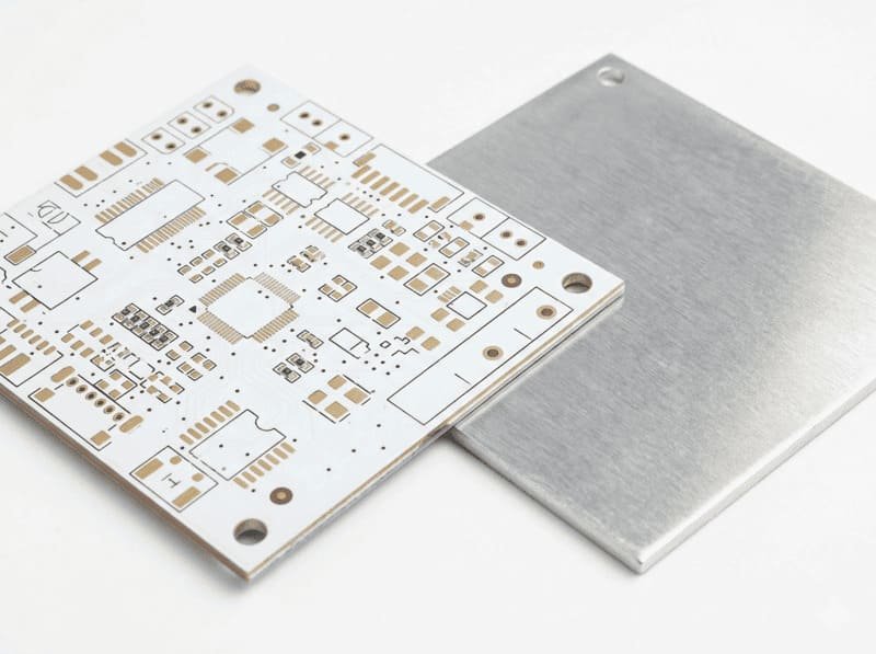
Aluminum PCB
- 1-2 layer designs
- 24 hour rapid production available
- Thickness options: 0.8mm-3.2mm
- Copper weights: 0.5-4oz
- Precision trace/spacing down to 3/3 mil
- Enhanced thermal dissipation
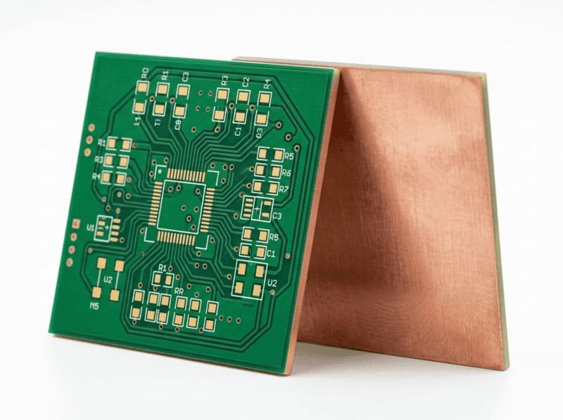
Copper Core PCB
- 1 - 2 layer configurations
- 1.0-2.0mm thickness options
- 1-2oz copper weights
- Superior thermal management properties
Ceramic PCB
- Layer count: 1-2 layers
- Turn time: from 24 hours
- Thickness: 0.8mm-3.2mm
- Copper: 0.5-4oz
- Min trace/spacing: 3/3 mil
Get Your Turnkey PCB Manufacturing Quote Within 12 Hours
Our experienced engineering team will analyze your requirements and provide a detailed production plan with transparent pricing.