Skip to content
 HDI PCB Manufacturer
The Backbone of Modern Electronics
What is HDI PCB?
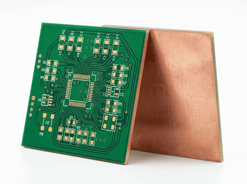
High Density Interconnect (HDI) PCB represents the cutting edge of circuit board manufacturing, enabling significantly higher connection density in a compact footprint. At LZJPCB, we define HDI PCBs as advanced circuit boards featuring microvias (typically less than 150μm in diameter), fine line width/spacing (under 100μm), and high connection pad density that exceeds conventional PCB capabilities.
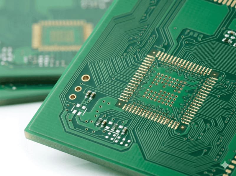
HDI technology uses a combination of laser drilled microvias, advanced lamination processes, and precision manufacturing techniques to create interconnections between layers that are significantly smaller than traditional mechanical drilling allows. This enables us to pack more functionality into smaller spaces, a critical advantage for today’s miniaturized electronic devices.
Working with many industrial automation clients, I’ve seen firsthand how HDI technology has transformed control systems by allowing more processing power and connectivity options in the same or smaller form factors. For industrial manufacturers like yours, this means more capable equipment without increasing size, an essential competitive advantage in modern factory environments.
What are the advantages of HDI PCB?
Enhanced Signal Integrity and Electrical Performance
HDI PCBs deliver superior signal integrity through shorter signal paths and reduced parasitic effects. With via in pad design and finer trace geometries, we achieve controlled impedance with ±7% tolerance even in high density layouts. This precision is critical for high speed industrial control systems where signal timing and quality directly impact operational reliability.
In a recent project for a German automation client, we reduced signal path lengths by 40% through HDI technology, eliminating intermittent communication issues that had plagued their previous conventional PCB design. Their equipment now maintains stable operation even in electrically noisy factory environments.
Significant Size and Weight Reduction
Our HDI manufacturing capabilities typically reduce PCB footprint by 30-50% compared to traditional designs. This remarkable space efficiency comes from: - Elimination of through holes that waste valuable routing space - Finer line/space geometries (down to 3/3 mil) - Higher layer count in thinner overall packages - Via in pad technology eliminating fan out space requirements For industrial equipment manufacturers, this translates to more compact control systems, sensors, and interface modules without sacrificing functionality or reliability. One of our industrial clients recently reduced their main controller board size by 35%, allowing them to offer a more compact machine that opened new market opportunities where installation space was limited.
Improved Thermal Management
Despite their higher component density, HDI PCBs often demonstrate better thermal performance through: - More efficient copper distribution with additional layers - Shorter thermal paths to dissipation points - Strategic placement of thermal vias under heat generating components - The ability to incorporate embedded heat sinks in critical areas Our thermal simulation capabilities ensure optimal heat distribution across your industrial control boards, preventing hotspots that can reduce component lifespan. This is particularly valuable for industrial systems operating continuously in elevated temperature environments.
What is HDI PCB commonly used in?
Modern industrial control systems demand increasing processing power and I/O density within space constrained environments. Our HDI PCBs enable:
- Higher processor performance with optimized signal routing
- More compact PLC and DCS modules with enhanced functionality
- Improved noise immunity through better ground plane implementation
- Enhanced thermal management for continuous operation
I recently worked with a leading German automation company to redesign their main controller board using HDI technology. The result was a 40% reduction in board size while adding additional communication interfaces and enhanced processing capabilities. Their new control system now offers industry leading functionality in a form factor that fits existing installation footprints.
The industrial IoT revolution demands intelligent devices at the network edge with significant processing capability and connectivity options:
- Complex multi radio wireless communication systems (WiFi, Bluetooth, cellular, LoRa)
- Edge processing units with advanced microprocessors and memory subsystems
- Sensor fusion modules integrating multiple data streams
- Low power designs with optimized power distribution
HDI technology is essential for these space constrained, feature rich devices. Our manufacturing capabilities support the fine pitch components and dense interconnections required for modern IoT edge devices deployed in industrial environments.
Advanced industrial sensing systems benefit significantly from HDI technology:
- Camera and imaging modules with high speed data interfaces
- Multi channel analog sensing with minimal crosstalk
- Precision measurement systems requiring optimal signal integrity
- High resolution displays and interface systems
The fine pitch capabilities of HDI are particularly valuable for sensor array connections and high speed image processing circuitry. For a machine vision client, we recently developed a 12 layer HDI board supporting sixteen parallel camera interfaces in a compact form factor that would have been impossible with conventional PCB technology.

HDI PCB Design Considerations

The selection of appropriate microvia technology significantly impacts both performance and manufacturability:
**Laser Drilled Microvias**: Our standard approach using CO₂ or UV lasers, capable of creating vias down to 75μm in diameter
**Photo Defined Microvias**: For ultra high density requirements with via diameters below 50μm
**Stacked vs. Staggered Microvias**: Offering different reliability profiles for various industrial operating environments
For industrial applications, I typically recommend staggered microvia designs over stacked configurations when possible, as they offer enhanced reliability under thermal cycling conditions common in factory environments. Our design engineers can guide you through these options based on your specific requirements.
The layer stack up in HDI PCBs requires careful planning to optimize both electrical performance and manufacturing reliability:
- Symmetrical construction to prevent warping during thermal cycles
- Controlled impedance layers for signal integrity
- Strategic placement of ground planes for EMI shielding
- Appropriate dielectric thicknesses between layers
Our engineering team designs custom stack ups for each industrial application, considering operating environment, signal integrity requirements, and thermal management needs. For a recent industrial automation client, we developed a 12 layer HDI stack up with embedded shielding layers that reduced electromagnetic interference by 85% in their motor control system.
To ensure manufacturing success and reliability in industrial applications, we recommend following these design guidelines:
1. Maintain aspect ratios below 0.8:1 for microvias to ensure reliable plating
2. Implement teardrops at via connections to enhance mechanical strength
3. Use adequate copper to dielectric adhesion promotion techniques
4. Ensure proper clearance between microvias and adjacent features
5. Consider thermal relief connections for components with high thermal loads
Our DFM review process identifies potential manufacturing issues early in the design phase, helping industrial clients avoid costly revisions and production delays. We provide detailed design rule recommendations tailored to your specific application requirements.
HDI PCB Types and Construction Methods
1+N+1 HDI Structure

The basic HDI structure features a conventional multilayer core with one HDI build up layer on each side. This construction offers an excellent balance of increased connection density and cost effectiveness, making it ideal for industrial control systems that need enhanced capabilities without extreme miniaturization.
At LZJPCB, we’ve optimized our 1+N+1 manufacturing process to minimize cost premiums over conventional PCBs while delivering significantly higher connection density. This makes it an excellent entry point for industrial automation manufacturers looking to upgrade their control system capabilities.
2+N+2 HDI Structure
For more demanding applications, our 2+N+2 structure provides two HDI build up layers on each side of a conventional core. This configuration enables much higher routing density and more complex interconnection schemes necessary for advanced industrial systems with numerous I/O requirements or high speed processing needs.
The additional build up layers provide greater design flexibility and improved signal integrity through more direct routing options. Several of our industrial clients have adopted this technology for their next generation control systems where processing density and communication bandwidth requirements have increased substantially.

Any Layer HDI

The most advanced HDI structure allows interconnections between any layers in the PCB stack up through staggered or stacked microvias. This construction enables the highest possible connection density for extremely complex industrial systems where maximum functionality must be packed into minimal space.
While typically more expensive than other HDI types, Any Layer HDI delivers unmatched design flexibility and miniaturization potential. This technology is increasingly adopted in sophisticated industrial applications like advanced robotics controllers, high resolution imaging systems, and complex sensor fusion modules.
HDI PCB Manufacturing Process at LZJPCB
Advanced Manufacturing Technologies

At our manufacturing facilities, we employ state of the art equipment specifically optimized for HDI production:
– **Precision Laser Drilling Systems**: Our ESI and Hitachi laser drilling systems achieve microvia diameter tolerance of ±20μm with exceptional positioning accuracy
– **Advanced Imaging Equipment**: LDI (Laser Direct Imaging) systems with 15μm line resolution capability
– **Sequential Lamination Presses**: Computer controlled lamination with ±25μm layer to layer registration
– **Automated Optical Inspection**: 100% inspection of microvia formation and trace integrity
These advanced manufacturing capabilities allow us to produce HDI PCBs with exceptional quality and consistency for industrial applications where reliability is paramount. Our continuous investment in manufacturing technology keeps us at the forefront of HDI capabilities.
Quality Control Measures

Our HDI PCB manufacturing incorporates comprehensive quality verification at every stage:
1. **Incoming Material Inspection**: Verification of critical material parameters
2. **Laser Drill Quality Verification**: Optical inspection of via diameter and positioning
3. **Cross Section Analysis**: Regular sampling for microvia formation quality
4. **Electrical Testing**: 100% test
ing with specialized flying probe equipment for fine pitch HDI
5. **3D X-Ray Inspection**: Internal layer registration and hidden feature verification
6. **Impedance Testing**: Verification of controlled impedance traces
These rigorous quality measures ensure that industrial clients receive HDI PCBs that meet or exceed IPC Class 2 and Class 3 requirements. For critical industrial applications, we can implement additional customized testing protocols to verify specific performance parameters.
Material Selection for Industrial HDI PCBs

We carefully select materials optimized for HDI applications in industrial environments:
– **High Performance Laminates**: Modified FR4, enhanced epoxy systems, and specialty materials with improved Tg (170°C+) and thermal stability
– **Low Loss Dielectrics**: For high frequency or high speed digital applications
– **Halogen Free Options**: Meeting environmental requirements without performance compromise
– **Thermally Enhanced Materials**: For applications with significant heat generation
For industrial clients operating in harsh environments, we recommend materials specifically formulated for enhanced reliability under thermal cycling, elevated temperatures, and environmental stress conditions. Our material scientists work with your team to select the optimal substrate for your specific application requirements.
LZJPCB HDI PCB Manufacturing Capabilities
| Features | Capabilities |
|---|---|
| Layer Count | Up to 32+ layers with precise registration |
| Minimum Line Width/Spacing | Down to 3/3 mil (75μm) standard, 2/2 mil (50μm) advanced |
| Board Thickness | 0.4mm to 3.2mm with ±10% tolerance |
| Microvia Diameter | Down to 0.10mm (4 mil) |
| Aspect Ratio | Up to 0.8:1 for reliable plating |
| Lamination Cycles | Up to 8 sequential laminations |
| Microvia Structures | Stacked, staggered, and combination designs |
| HDI Types | 1+N+1, 2+N+2, Any-Layer HDI |
| Surface Finish Options | ENIG, Immersion Silver, Immersion Tin, OSP, HASL, Hard Gold |
| Controlled Impedance | ±7% tolerance for critical traces |
| Advanced Features | Embedded components, cavity designs, hybrid material stack-ups |
| IPC Compliance | IPC-6016 Class 2 standard, Class 3 available |
| Testing | 100% electrical testing, impedance verification, AOI, X-ray inspection |
| Quality Systems | ISO 9001:2015, ISO 13485, IATF 16949 compliant processes |
| Typical Lead Times | Prototype: 3-5 days, Standard: 7-10 days, Volume: 10-15 days |
Why Choose LZJPCB for HDI PCB
Technical Expertise and Design Support
Our engineering team brings decades of combined HDI manufacturing experience: - Dedicated HDI design review experts to optimize your designs - Stackup design assistance for optimal electrical and thermal performance - DFM consultation to ensure manufacturing reliability - Signal integrity analysis for critical high speed circuits This expertise translates into higher first pass success rates and reduced time to market for your industrial products. We don't just manufacture boards, we partner with your team to ensure optimal design implementation for your specific application requirements.
Manufacturing Excellence
Our dedicated HDI manufacturing lines feature: - Tightly controlled processes with comprehensive statistical process control - Advanced equipment calibrated specifically for HDI requirements - Cleanroom environments for critical process steps - Rigorous testing protocols exceeding industry standards These manufacturing advantages ensure consistent quality and reliability across production runs, a critical factor for industrial equipment manufacturers who need consistent performance from every unit they produce.
Global Supply Chain Capabilities
With manufacturing facilities in both China and Indonesia, we offer exceptional flexibility: - Regional production options to meet specific export requirements - Robust supply chain resilience through facility diversification - Optimized logistics for different global markets - Consistent quality standards across all manufacturing locations For multinational industrial clients, our global footprint provides valuable supply chain flexibility while maintaining consistent quality standards. As you expand into North American and Asia Pacific markets, our regional production capabilities can help optimize your logistics and reduce lead times.
HDI PCB FAQ
What is the typical cost difference between conventional PCBs and HDI PCBs?
HDI PCBs generally cost 15-40% more than conventional PCBs with similar layer counts, depending on design complexity and volume. However, this direct cost comparison overlooks significant value advantages:
1. HDI often enables higher component density, potentially reducing board size by 30-50%
2. Smaller board dimensions reduce overall material costs across your product
3. Enhanced performance may eliminate the need for additional components or filtering
4. Improved reliability can reduce warranty and service costs
5. Smaller end products may open new market opportunities
For industrial clients, we conduct comprehensive cost benefit analysis to determine if HDI technology delivers overall value. In many cases, the performance and miniaturization benefits justify the moderate cost premium. For high volume production, we implement specific cost optimization strategies to minimize the HDI premium while maintaining performance advantages.
What are the reliability considerations for HDI PCBs in industrial environments?
HDI PCBs designed and manufactured properly offer excellent reliability for industrial applications. Key considerations include:
**Thermal Cycling Endurance**: Our HDI designs implement stress relieving features around microvias to withstand the repeated thermal cycles common in industrial equipment
**Vibration Resistance**: Fine HDI traces may require additional design considerations in high vibration environments
**Environmental Protection**: For harsh industrial settings, we recommend appropriate conformal coating or encapsulation
**Long Term Reliability**: Our HDI manufacturing processes are optimized for long service life (10+ years) required by industrial equipment
We conduct reliability testing including thermal cycling, vibration analysis, and accelerated life testing for critical industrial applications. For clients with specific reliability concerns, we can implement customized testing protocols to validate performance under their exact operating conditions.
How do lead times for HDI PCBs compare to conventional PCBs?
HDI PCBs typically require additional processing steps compared to conventional PCBs, resulting in moderately longer lead times:
**Prototype HDI PCBs**: 3-5 business days (vs. 1-3 days for conventional)
**Medium Volume Production**: 7-10 business days (vs. 5-7 days for conventional)
**High Volume Production**: 10-15 business days (vs. 8-12 days for conventional)
For industrial clients with scheduled production requirements, we offer dedicated capacity allocation programs that ensure consistent delivery timelines aligned with your production schedule. Our dual manufacturing locations provide additional flexibility to accommodate urgent requirements when needed.
What design tools and file formats do you support for HDI PCB manufacturing?
We support all major EDA platforms and file formats:
– **Design Software**: Altium Designer, Cadence Allegro, Mentor Pads, Eagle, KiCad, and others
**Data Formats**: Gerber (RS-274X), ODB++, IPC-2581, and native CAD files
**Documentation**: We accept specifications in PDF, Excel, and standard document formats
Our engineering team can work with your design files in virtually any format, converting as needed for our manufacturing systems. For complex HDI designs, we recommend ODB++ or IPC-2581 formats as they contain the most comprehensive design information.
How do you ensure quality and consistency for HDI PCBs?
Our HDI quality assurance system includes:
1. **Advanced Inspection Equipment**: AOI, AXI, and advanced microscopy systems specifically calibrated for HDI feature sizes
2. **Comprehensive Testing**: 100% electrical testing with specialized flying probe equipment for fine pitch HDI
3. **Statistical Process Control**: Continuous monitoring of critical HDI parameters with closed loop feedback
4. **Cross Section Analysis**: Regular destructive testing of production samples to verify internal quality
5. **Material Traceability**: Complete tracking of all materials used in HDI construction
6. **Certified Staff**: Specialized training for all technicians involved in HDI production
For industrial clients with mission critical applications, we offer enhanced quality documentation including detailed inspection reports, material certifications, and process verification data. Our quality systems are designed to meet IPC Class 3 requirements when specified.
Unlock More Possibilities with LZJPCB Solutions
From advanced HDI PCBs to specialized flex-rigid boards, our manufacturing services deliver exceptional quality across diverse technologies and applications tailored for industrial automation requirements.
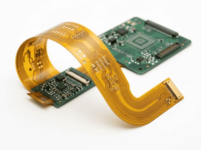
Flex PCB
- Layer count: 1-32 layers
- Turn time: from 24 hours
- Thickness: 0.4mm-4.0mm
- Copper: 1-15oz
- Min trace/spacing: 3/3 mil
HDI PCB
- 4-20 layer HDI designs
- Advanced buried and blind via technology
- 10 day production timeline
- Ideal for complex, space constrained applications
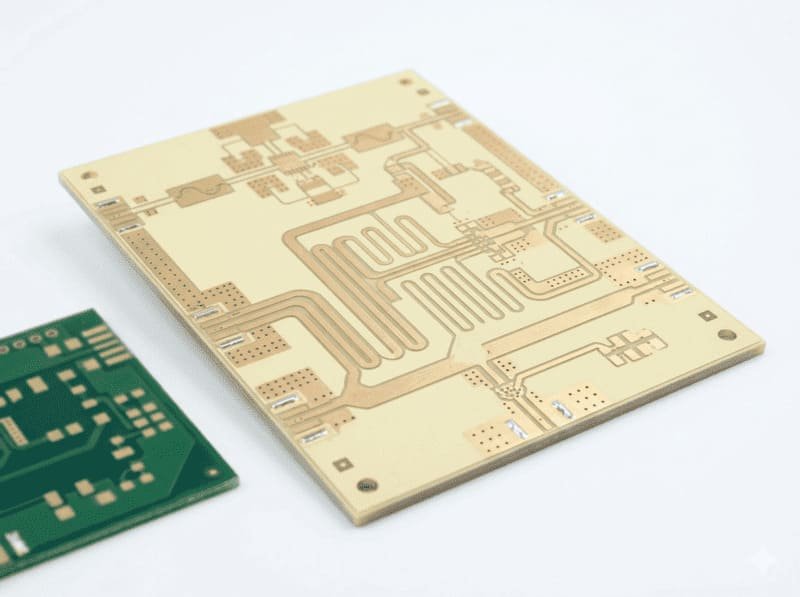
Rogers PCB
- 5 day production timeline
- Premium RO4003C and RO4350B materials
- Specialized for RF and high frequency applications
- Exceptional signal integrity performance
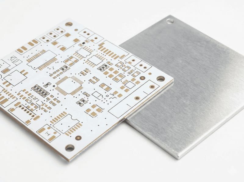
Aluminum PCB
- 1-2 layer designs
- 24 hour rapid production available
- Thickness options: 0.8mm-3.2mm
- Copper weights: 0.5-4oz
- Precision trace/spacing down to 3/3 mil
- Enhanced thermal dissipation
Copper Core PCB
- 1 - 2 layer configurations
- 1.0-2.0mm thickness options
- 1-2oz copper weights
- Superior thermal management properties
Ceramic PCB
- Layer count: 1-2 layers
- Turn time: from 24 hours
- Thickness: 0.8mm-3.2mm
- Copper: 0.5-4oz
- Min trace/spacing: 3/3 mil
Get Your Turnkey PCB Manufacturing Quote Within 12 Hours
Our experienced engineering team will analyze your requirements and provide a detailed production plan with transparent pricing.