Skip to content
 Every electronic device you’ve ever used contains a hidden world of complexity. Behind those sleek exteriors lies a bewildering array of components that must connect perfectly, or nothing works at all.
PCB assembly (PCBA) is the process of attaching electronic components to a bare printed circuit board to create a functional electronic circuit. This involves component placement, soldering, inspection, and testing to transform an unpopulated PCB into a working electronic assembly that powers devices.
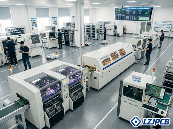
The assembly process is where PCBs come to life. As a manufacturing engineer, I’ve overseen thousands of PCB assemblies, from simple single layer boards to complex multilayer designs with thousands of components. Understanding this process is critical whether you’re designing electronics, sourcing manufacturing, or simply trying to understand how your devices work. Let’s explore the key aspects of PCB assembly and why it matters so much in electronics manufacturing.
What is the Main Purpose of a PCB?
Have you ever wondered how all those tiny electronic components work together? Without PCBs, our modern electronic devices wouldn’t exist in their current compact, reliable forms.
The main purpose of a PCB is to mechanically support and electrically connect electronic components using conductive pathways etched from copper sheets laminated onto a non conductive substrate. This creates a reliable, organized platform that enables complex electronic functions while minimizing size and weight.
PCBs serve as the backbone of nearly every electronic device we use today. I remember my first electronics project in university, attempting to build a simple circuit using just wires and a breadboard. The result was a mess of connections that barely worked and fell apart when touched. This experience gave me a deep appreciation for what PCBs accomplish.
The Essential Functions of PCBs
PCBs have revolutionized electronics manufacturing since their introduction. Before PCBs became standard, electronics relied on point to point wiring, which was labor intensive, error prone, and resulted in bulky, unreliable products. The development of the PCB changed everything about how we design and produce electronic devices.
| Function | Description | Impact on Electronics |
|---|---|---|
| Electrical Connectivity1 | Creates pathways for electrical signals between components | Enables complex circuit designs in minimal space |
| Mechanical Support | Provides stable mounting platform for components | Increases durability and shock resistance |
| Heat Dissipation2 | Helps distribute and remove heat from components | Improves reliability and component lifespan |
| Signal Integrity | Maintains proper electrical characteristics for signals | Enables higher speed operation and reduces interference |
| Component Organization3 | Standardizes component layout and connections | Facilitates automated assembly and testing |
Beyond these core functions, PCBs have evolved to serve additional purposes. Modern PCBs often include features like impedance control for high frequency applications4, embedded components to save space, and specialized materials for thermal management or flexibility.
The importance of PCBs extends beyond just making connections. They also serve as documentation of the circuit design itself. The physical layout of traces and components on a PCB represents the circuit schematic in a tangible form, making it easier to understand, troubleshoot, and modify designs.
In my work at LZJPCB, I’ve seen how critical proper PCB design is for product success. A well designed PCB doesn’t just connect components—it optimizes performance, reliability, manufacturability, and cost. This is why companies invest significant resources in PCB design and why choosing the right manufacturing partner is crucial.
What Are the Three Types of PCBs?
When I first entered the electronics industry, I was surprised by the variety of PCBs available. The differences between them significantly impact product performance, cost, and reliability.
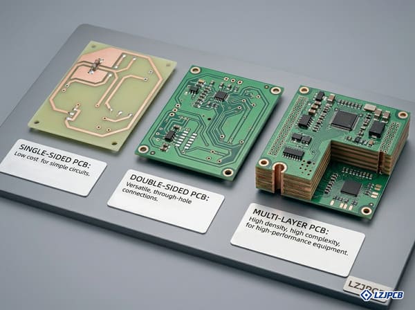
The three main types of PCBs are single sided PCBs with components and traces on one side only, double sided PCBs with components and traces on both sides, and multilayer PCBs with multiple layers of conductive traces separated by insulating materials and connected through vias.
The evolution of PCB technology has closely followed the increasing complexity of electronic devices. Each type of PCB serves different applications and comes with its own advantages and limitations. Understanding these differences helps in selecting the most appropriate board type for specific project requirements.
Comparing PCB Types by Structure and Application
The choice of PCB type depends on several factors including circuit complexity, space constraints, performance requirements, and budget considerations. I’ve worked with clients across multiple industries, and the selection process always comes down to finding the right balance between these factors.
| PCB Type | Structure | Typical Applications | Advantages | Limitations |
|---|---|---|---|---|
| Single sided | Components on one side, traces on opposite side | Simple electronics, calculators, radios, power supplies | Lowest cost, easiest to design and manufacture, good for high volume production | Limited circuit density, not suitable for complex circuits |
| Double sided | Components and traces on both sides, connected by vias | Consumer electronics, industrial controls, instrumentation | Better circuit density than single sided, reasonable cost, good heat dissipation | More complex manufacturing, higher cost than single sided |
| Multilayer | 4+ conductive layers with insulating substrates | Smartphones, computers, medical devices, aerospace equipment | Highest circuit density, best for complex designs, superior signal integrity | Most expensive, longer manufacturing time, more complex design process |
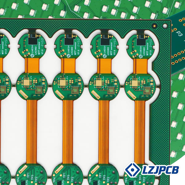
Beyond these three basic types, there are specialized variants that serve particular needs. Flexible PCBs can bend or fold to fit unusual spaces. Rigid flex PCBs combine rigid and flexible sections for applications that need both stability and flexibility. High frequency PCBs use special materials optimized for RF performance. Metal core PCBs incorporate a metal layer for enhanced heat dissipation.
In recent years, I’ve seen increasing demand for HDI (High Density Interconnect) PCBs, which use advanced manufacturing techniques to achieve finer traces and smaller vias. These allow for more components in a smaller area, which is essential for modern compact devices like smartphones and wearables.
The choice of PCB type is one of the earliest and most consequential decisions in electronics design. It affects every subsequent aspect of the project from component selection to manufacturing processes. At LZJPCB, we often consult with clients early in their design process to ensure they select the most appropriate PCB type for their specific requirements and constraints.
Why is it Called a PCB?
The term PCB is so common in electronics that we rarely stop to consider its origin. But understanding the name helps clarify what these devices actually are and how they function.
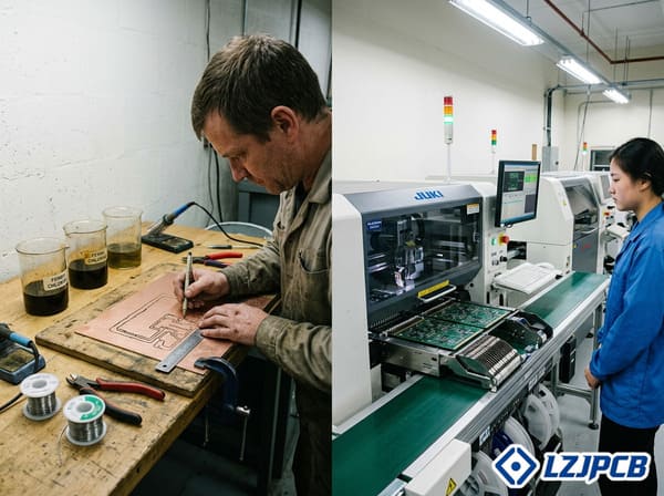
PCB stands for "Printed Circuit Board" because the circuit connections are "printed" using techniques similar to traditional printing methods. Originally, conductive ink was literally printed onto the board, though modern manufacturing uses photolithography and etching to create the copper traces.
The name has remained despite significant changes in how PCBs are actually manufactured. The concept of "printing" electrical pathways has been fundamental to electronics manufacturing since the early 20th century, though the techniques have evolved dramatically.
The Evolution of PCB Terminology and Manufacturing
The history of PCBs reflects broader technological evolution. Each advancement in materials, design techniques, and manufacturing processes has enabled more complex and capable electronic devices. I find this history fascinating because it shows how innovation in manufacturing processes directly enables new product possibilities.
| Era | Terminology | Manufacturing Method | Key Characteristics |
|---|---|---|---|
| 1920s-1940s | "Printed Wiring" | Actual printing with conductive inks | Simple patterns, limited durability |
| 1950s-1960s | "Printed Circuit" | Photoengraving and etching | More precise, better durability |
| 1970s-1980s | "PCB" standardized | Photolithography, screen printing | Multiple layers, plated through holes |
| 1990s-2000s | "PCB" continues | Computer controlled manufacturing, finer traces | Surface mount technology dominates |
| 2010s-Present | "PCB" with qualifiers (HDI PCB, Flex PCB, etc.) | Laser direct imaging, plasma etching | Microvias, embedded components, advanced materials |
The term "printed" in PCB reflects the fundamental process of transferring a pattern to a substrate, which remains conceptually similar despite technological advances. Early PCBs were indeed produced using methods adapted from the printing industry, where conductive patterns were literally printed onto insulating materials.
Today’s manufacturing processes are far more sophisticated. At LZJPCB, our manufacturing lines use computer controlled equipment that creates traces with microscopic precision. Modern PCBs are produced using a combination of photolithography5, chemical etching, mechanical drilling, plating, and other processes that would be unrecognizable to early PCB pioneers.
Despite these changes, the name "Printed Circuit Board6" has persisted because it effectively communicates the essential function: creating predetermined electrical pathways on a board. The industry has added qualifiers to describe specific types (like "flexible PCB7" or "high frequency PCB"), but the base terminology remains unchanged.
This consistency in terminology has been helpful as the electronics industry has globalized. Whether you’re working with manufacturers in China, Europe, or North America, the term PCB is universally understood, facilitating communication across language barriers and technical specialties.
Conclusion
PCB assembly transforms bare circuit boards into functional electronic systems by mounting and soldering components. The process bridges PCB design and working electronic products, with modern assemblies using advanced techniques like SMT for increasingly complex, compact devices in our technology driven world.
-
Learn how electrical connectivity enables complex circuit designs, crucial for modern electronics. ↩
-
Discover how effective heat dissipation enhances reliability and lifespan of electronic components. ↩
-
Understanding component organization can improve assembly efficiency and reduce errors in production. ↩
-
Delve into this advanced feature to see how it impacts performance in high speed electronics. ↩
-
Explore the photolithography process to see how it revolutionizes PCB production and enhances precision. ↩
-
Understanding the definition of PCB is crucial for grasping its role in electronics and manufacturing. ↩
-
Explore the innovative world of flexible PCBs and their diverse applications in today’s technology. ↩