Skip to content
 Electronics manufacturers often confuse PCB and PCBA terms when communicating with suppliers, leading to costly misunderstandings, incorrect quotes, delayed projects, and products that don’t meet specifications. This confusion impacts budgeting, timelines, and ultimately, product success.
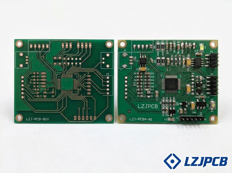
A PCB (Printed Circuit Board) is the bare fiberglass board with copper traces, holes, and pads but no components attached. A PCBA (Printed Circuit Board Assembly) is a PCB with all electronic components soldered onto it, creating a functional electronic circuit ready for installation into a final product.
Understanding the difference between PCB and PCBA is fundamental to working effectively in the electronics manufacturing industry. At LZJPCB, I regularly help clients navigate these distinctions to ensure they’re ordering exactly what they need. The confusion between these terms goes beyond simple semantics – it affects project planning, budgeting, and production timelines. Let me clarify the key differences and help you understand which service you actually need for your electronics project.
Is PCB Assembly An Embedded System?
Many engineers and project managers struggle to correctly classify their electronic products, leading to miscommunications with manufacturers, incorrect component selection, and development approaches that don’t align with project requirements. This confusion extends to whether PCB assemblies qualify as embedded systems1.
PCB assembly is not inherently an embedded system, but rather the physical manufacturing process that can create embedded systems. An embedded system specifically requires a microcontroller or processor running dedicated software to perform specific functions, while many PCB assemblies may be simple analog circuits without programmable components.
This distinction is important for properly classifying and approaching electronic product development. At LZJPCB, we produce both simple PCB assemblies and complex embedded systems1, and understanding the difference helps us provide the right manufacturing support for each project type. Let me explain the relationship between these concepts in more detail.
Understanding PCB Assembly and Embedded Systems
The relationship between PCB assemblies and embedded systems1 involves important distinctions and overlaps. Based on my experience manufacturing various electronic products, I can clarify these concepts and their practical implications.
| Aspect | PCB Assembly (PCBA) | Embedded System | Relationship |
|---|---|---|---|
| Definition | Physical process of mounting and soldering components onto a PCB | Computing system with dedicated function within a larger mechanical or electrical system | An embedded system is typically implemented as a PCBA, but not all PCBAs are embedded systems1 |
| Core Components | May include any electronic components (passive components, ICs, connectors, etc.) | Requires microcontroller2/processor, memory, I/O interfaces | Embedded systems are a subset of PCBAs with specific computing capabilities |
| Programming | Not necessarily programmable | Requires firmware3/software | Programming is essential for embedded systems1 but not for all PCBAs |
| Functionality | Can range from simple circuits to complex systems | Performs dedicated computing functions with specific inputs/outputs | Embedded system functionality is determined by both hardware (PCBA) and software |
| Examples | Power supplies, amplifiers, sensor interfaces4, embedded systems1 | Smart thermostats, automotive control units, medical devices | All embedded systems1 include PCBAs, but many PCBAs (like power supplies) are not embedded systems1 |
| Development Process | Electronics design, layout, manufacturing | Electronics design, layout, manufacturing + software development | Embedded systems require additional development steps beyond PCBA manufacturing |
PCB Assembly (PCBA) refers specifically to the manufacturing process of attaching components to a printed circuit board. This process typically includes:
- Applying solder paste to the bare PCB
- Placing components onto the board using pick and place machines
- Reflow soldering to create permanent connections
- Inspection and testing of the assembled board
- Any additional processes like conformal coating5 or potting
The result of PCB assembly6 is a functional electronic circuit, but this circuit may serve various purposes. Some PCBAs perform simple functions without any programmable elements, such as:
- Power supply circuits
- Audio amplifiers
- Signal conditioning circuits
- Passive filter networks
- LED lighting controllers
- Simple timing circuits
These types of PCBAs are not embedded systems1 because they lack programmable intelligence and operate based on fixed electronic principles rather than software instructions.
An embedded system, by contrast, is specifically a computing system designed to perform dedicated functions within a larger mechanical or electrical system. The key characteristics that define an embedded system include:
- A microcontroller2 or processor as the central component
- Memory for storing program instructions and data
- Input/output interfaces to interact with the external world
- Software/firmware3 that defines its functionality
- Dedicated purpose rather than general purpose computing
- Often real time operation requirements
- Usually integrated within a larger product or system
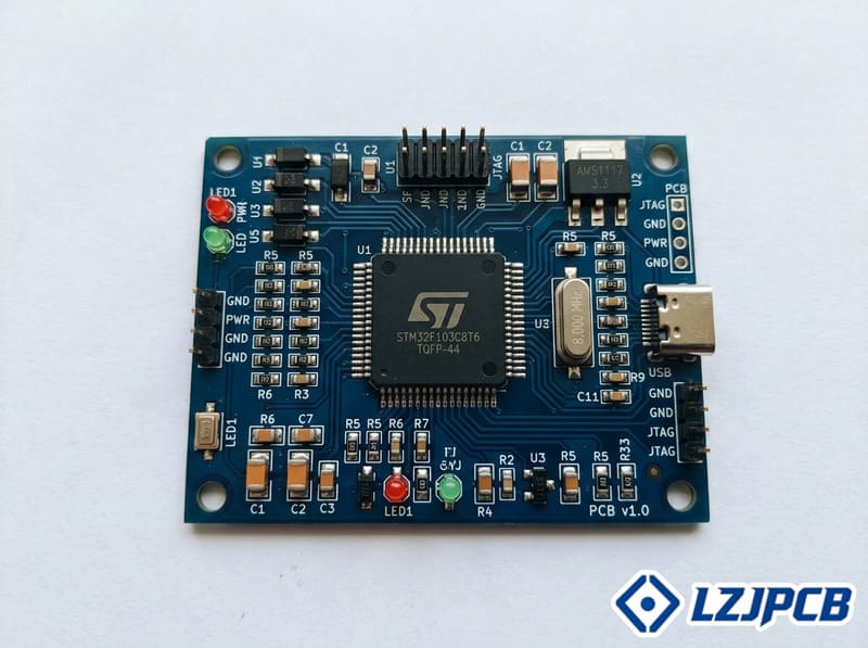
When we manufacture embedded systems1 at LZJPCB, the PCBA is essentially the physical implementation of the embedded system’s hardware layer. The board typically includes:
- The microcontroller2 or processor (the "brain")
- Memory components (both program and data storage)
- Various interface circuits for connecting sensors and actuators
- Power regulation components
- Communication interfaces (like UART, SPI, I2C, Ethernet, or wireless)
- Clock generation circuits
- Supporting passive components
What transforms this PCBA into an embedded system is the software loaded into the microcontroller2 or processor. This software, often called firmware3, provides the intelligence and specific functionality. Without this software, the PCBA would simply be an inert collection of components.
I recently worked with a client who was developing a smart irrigation controller. The PCBA we manufactured included a microcontroller2, memory, sensor interfaces4, relay drivers for valves, and a wireless module. This PCBA alone couldn’t function as an irrigation controller—it required the firmware3 our client developed to interpret sensor data, make watering decisions, and control the valves based on schedules and environmental conditions. The combination of the PCBA and firmware3 created the embedded system.
The development process also highlights the difference between general PCBAs and embedded systems1:
- For simple PCBAs, the development process focuses on circuit design7, component selection, PCB layout, and manufacturing.
- For embedded systems1, these same steps are required, but they’re followed by firmware3 development, debugging, and system integration.
This distinction has important implications for project planning and manufacturing:
-
Testing requirements: Simple PCBAs might only need electrical testing to verify connections and basic functionality. Embedded systems require more complex functional testing that exercises the software functions.
-
Development timeline: Embedded systems typically have longer development cycles due to the additional software development and integration phases.
-
Revision cycles: Embedded systems often go through more design iterations as both hardware and software evolve.
-
Manufacturing considerations: For embedded systems1, the manufacturing process may include programming8 steps to load firmware onto the devices.
-
Debugging complexity: Issues in embedded systems1 can stem from hardware problems, software bugs, or interactions between the two, making troubleshooting more complex.
In our manufacturing experience, we’ve observed that approximately 60-70% of the PCBAs we produce qualify as embedded systems1, with the remainder being non programmable circuits. This ratio has been steadily shifting toward embedded systems1 as more products incorporate "smart" features and connectivity.
The evolution of electronics has actually blurred these lines somewhat. Components that were once purely analog or non programmable (like power supplies or LED drivers) now often incorporate microcontrollers for advanced features like digital control, communication, or power management. This trend means that more PCBAs are becoming embedded systems1, even in applications that traditionally used simple analog circuits.
From a manufacturing perspective, embedded systems1 typically present additional challenges:
-
Component handling: Processors and memory chips often require more careful handling due to ESD sensitivity and fine pitch connections.
-
Programming and testing: In circuit programming8 may be required during or after assembly.
-
Traceability requirements: Embedded systems in regulated industries (medical, automotive, aerospace) often have stricter traceability requirements9 for both components and processes.
-
Conformal coating considerations: Many embedded systems1 require conformal coating5 for environmental protection, but this coating must be carefully applied to avoid covering programming8 interfaces or components that must remain accessible.
Understanding whether your project is a simple PCBA or an embedded system helps ensure appropriate planning, testing, and manufacturing approaches. It also affects how you communicate with your manufacturing partner about your project requirements.
What Is The Purpose Of A PCB?
Electronic product developers sometimes focus too narrowly on components and software, underestimating the critical role of the PCB10 itself. This oversight can lead to reliability problems, electromagnetic interference issues, and thermal management11 failures that compromise product performance and longevity.
A PCB’s purpose is to mechanically support and electrically connect electronic components using conductive traces, pads, and features etched from copper layers laminated onto a non conductive substrate. Beyond simple connectivity, PCBs provide physical structure, thermal management, electromagnetic interference (EMI) control, and signal integrity for electronic devices.
After manufacturing thousands of PCBs at LZJPCB12, I’ve gained a deep appreciation for how these seemingly simple boards serve complex functions beyond just connecting components. PCBs represent an incredible engineering achievement that we often take for granted. Let me explain the multiple roles PCBs play in modern electronics and why their proper design is critical to product success.
The Multifaceted Functions of Printed Circuit Boards
PCBs serve numerous vital functions in electronic devices, each contributing to overall product performance, reliability, and manufacturability. Based on my experience with diverse applications across industries, I can elaborate on these critical functions.
| Function | Description | Design Considerations | Examples |
|---|---|---|---|
| Electrical Connectivity | Creates conductive pathways between components | Trace width, spacing, impedance control | Signal routing, power distribution13 networks |
| Mechanical Support | Provides physical structure for mounting components | Board thickness, material strength, mounting points | Enclosure fit, component support, vibration resistance14 |
| Thermal Management | Dissipates heat from components | Copper pours, thermal vias15, substrate materials | Power converters, high performance processors |
| Signal Integrity | Maintains clean signal transmission | Controlled impedance, length matching, crosstalk minimization16 | High speed digital interfaces, RF circuits |
| EMI/EMC Control | Manages electromagnetic emissions and susceptibility | Ground planes, shielding, layout partitioning | Wireless devices, sensitive analog circuits |
| Size Reduction | Enables miniaturization of electronic devices | Component density, layer count, microvias | Consumer electronics, medical implants |
| System Organization | Groups related functions and interfaces | Circuit partitioning, connector placement | Complex multi function devices |
Electrical Connectivity
The primary function of PCBs is to provide electrical connections between components. This might seem straightforward, but modern PCBs accomplish this with remarkable sophistication:
-
Multi layer connectivity: Contemporary PCBs typically contain 2-16 layers (though I’ve worked on boards with up to 32 layers for complex telecommunications equipment). These layers allow for complex routing patterns that would be impossible in single plane wiring.
-
Controlled impedance: For high speed signals, PCBs maintain precise trace geometries and relationships to ground planes17 to ensure specific impedance values (typically 50Ω, 75Ω, 90Ω, or 100Ω depending on the application).
-
Power distribution: Beyond simple connections, PCBs include complex power distribution13 networks with plane layers that minimize voltage drops and provide low impedance power delivery.
-
Differential pairs: Modern high speed interfaces like USB, HDMI, and Ethernet require precisely matched differential pairs18 that maintain exact length matching and coupling characteristics throughout their path.
At LZJPCB, we recently manufactured a board for a telecommunications client that included over 15,000 individual connections across 14 layers. The copper traces, if laid end to end, would stretch more than half a kilometer, yet all were precisely packed into a board smaller than a standard sheet of paper.
Mechanical Support
PCBs provide the physical structure for electronic assemblies:
-
Component mounting: PCBs offer a stable platform for mounting components with precisely positioned pads and holes that align with component terminations.
-
Structural integrity: The fiberglass reinforcement in FR4 (the most common PCB10 material) provides excellent strength to weight ratio and dimensional stability across varying environmental conditions.
-
System integration: PCBs include mounting holes, edge connectors, and mechanical features that allow them to be properly integrated into larger systems and enclosures.
-
Vibration and shock resistance: Properly designed PCBs can withstand significant mechanical stress, crucial for applications like automotive electronics or industrial equipment.
One of our industrial clients relies on PCBs that must withstand continuous vibration in factory environments. The boards include additional mounting points, thicker substrates (2.4mm vs. the standard 1.6mm), and component adhesive reinforcement to ensure reliability under these demanding conditions.
Thermal Management
Modern electronic components generate significant heat that must be managed to ensure reliability and performance:
-
Heat spreading: Copper layers in PCBs help distribute heat away from hot components, reducing localized hot spots.
-
Thermal vias: Arrays of small vias transfer heat between layers and can connect to internal or external heat sinking structures.
-
Substrate selection: Materials with higher thermal conductivity can be selected for high power applications.
-
Component placement optimization: PCB10 layout can strategically position heat generating components to optimize thermal dissipation.
We recently produced PCBs for high brightness LED lighting systems where thermal management11 was the primary design consideration. The boards used thick copper (3oz, compared to standard 1oz) and hundreds of thermal vias6 to efficiently transfer heat from the LED components to the attached heatsink.
Signal Integrity
As electronic devices operate at increasingly higher speeds, PCBs play a crucial role in maintaining signal integrity19:
-
Impedance control: By carefully controlling trace width, spacing from ground planes17, and dielectric properties, PCBs maintain consistent impedance along signal paths to prevent reflections and signal degradation.
-
Length matching: For parallel interfaces and differential pairs18, PCBs incorporate precise trace length matching (sometimes down to 0.1mm tolerance) to ensure signals arrive simultaneously.
-
Crosstalk minimization: PCB10 layout techniques separate sensitive signals, incorporate guard traces, and use ground planes17 to minimize interference between adjacent signals.
-
Via design: Signal transitions between layers are carefully designed to minimize impedance discontinuities that could degrade high speed signals.
One of our telecommunications customers requires PCBs that maintain signal integrity19 for 56Gbps SerDes interfaces. These boards require extraordinary attention to material selection, layer stackup design, and trace geometry to preserve signal quality at these extreme speeds.
EMI/EMC Control
PCBs play a critical role in managing electromagnetic emissions and susceptibility:
-
Ground planes: Continuous ground planes17 provide low impedance return paths for signals and power, reducing loop areas that could act as antennas.
-
Circuit partitioning: PCBs can physically separate sensitive analog circuits from noisy digital sections to minimize interference.
-
Filtering and decoupling: PCBs incorporate power filtering structures and provide mounting for decoupling capacitors that reduce noise.
-
Shielding integration: Many PCBs include provisions for attaching EMI shields or incorporate ground "fences" of vias around sensitive circuits.
We produced PCBs for a medical device manufacturer where EMI control20 was critical to prevent interference with other hospital equipment. The design included separate analog and digital ground planes17, extensive filtering, and careful stackup design to minimize emissions while ensuring immunity to external interference sources.
Size Reduction
PCBs enable the remarkable miniaturization of modern electronics:
-
Component density: Modern PCBs can place thousands of components in extremely compact arrangements.
-
Microvias and HDI: High Density Interconnect (HDI) techniques using laser drilled microvias allow for more connections in smaller spaces.
-
Fine pitch components: PCBs provide the precision required to connect components with extremely fine lead spacing (down to 0.3mm or less).
-
3D integration: Rigid flex PCBs and board to board connectors allow electronics to be folded into compact three dimensional arrangements.
One of our consumer electronics clients recently transitioned from a traditional PCB10 to an HDI design, reducing board area by 40% while adding functionality. This allowed them to create a more compact product without compromising performance.
System Organization
PCBs help organize complex electronic systems:
-
Functional blocks: Related circuits can be grouped together on the PCB10 to improve signal integrity19 and simplify design understanding.
-
Interface standardization: PCBs incorporate standardized connectors and interfaces in appropriate locations.
-
Modular design: Complex systems can be divided across multiple PCBs that connect through standardized interfaces.
-
Design for test: PCBs can incorporate test points, boundary scan chains, and debug interfaces that make testing and troubleshooting more efficient.
We recently manufactured a modular industrial control system consisting of five interconnected PCBs, each handling different functions (power, processing, inputs, outputs, and communications). This modular approach allowed our client to customize systems for different customers by including only the required boards.
Beyond these primary functions, PCBs serve additional specialized purposes depending on the application:
-
Environmental protection: With appropriate materials and conformal coatings, PCBs can protect electronics in harsh environments with extreme temperatures, humidity, or corrosive substances.
-
Safety isolation: PCBs can incorporate creepage and clearance distances between high and low voltage circuits to ensure electrical safety.
-
Regulatory compliance: PCB10 design features support compliance with standards like UL, CE, and FCC requirements.
-
Tamper evidence/security: Some PCBs include security measures like buried traces, tamper evident coatings, or encrypted components to protect intellectual property.
-
Aesthetics: For consumer products where the PCB10 is visible, boards may serve aesthetic purposes with custom colors, logos, or specific surface finishes.
The sophistication of modern PCBs continues to evolve. We’re now seeing advanced features like:
- Embedded components (resistors and capacitors built inside the PCB10 layers)
- Integrated antennas for wireless communications
- Mixed rigid-flex construction for space constrained applications
- Specialized materials for extreme environments or high frequencies
- Additive manufacturing techniques that enable new geometries and capabilities
PCB vs. PCBA: Understanding the Key Differences
The distinction between PCB and PCBA represents a fundamental concept in electronics manufacturing. Based on my manufacturing experience, I can outline the comprehensive differences between these related but distinct terms.
Comparing PCB and PCBA: Manufacturing, Function, and Application
PCBs and PCBAs represent different stages in the electronics production process, each with distinct characteristics, requirements, and applications. Understanding these differences helps in properly planning, budgeting, and communicating about electronics projects.
| Characteristic | PCB (Printed Circuit Board) | PCBA (Printed Circuit Board Assembly) |
|---|---|---|
| Definition | Bare board with conductive tracks and pads | Completed electronic assembly with components |
| Manufacturing Process21 | Etching, drilling, plating, solder mask application | Component placement, soldering, cleaning, testing |
| Functionality | No electrical function on its own | Performs intended electronic functions |
| Testing Methods | Electrical continuity, impedance testing | Functional testing22, in circuit testing |
| Visual Appearance | Flat board with visible traces and pads | Board populated with various components |
| Manufacturing Time | Typically 1-15 days depending on complexity | Additional 1-10 days beyond PCB manufacturing |
| Cost Factors | Material, layer count, size, features | All PCB costs plus components and assembly labor |
| Design Files Required | Gerber files, drill files, fabrication drawings | All PCB files plus BOM, assembly drawings, pick and place data |
Manufacturing Process Differences
The PCB manufacturing process creates the bare board and typically includes:
- Design and engineering: Creating the PCB layout using CAD software
- Film generation: Producing photographic films of each layer (though many manufacturers now use direct imaging)
- Substrate preparation: Cutting the base material (typically FR4) to size
- Inner layer processing: Printing and etching the internal copper layers
- Layer alignment and lamination: Pressing the layers together with prepreg (pre impregnated epoxy glass)
- Drilling: Creating holes for vias and through hole components
- Plating: Depositing copper in the drilled holes to create electrical connections between layers
- Outer layer imaging and etching: Creating the external copper patterns
- Solder mask application: Applying the protective coating (typically green, but available in various colors)
- Surface finish: Applying finish like HASL, ENIG, or OSP to protect exposed copper and ensure solderability
- Silkscreen printing: Adding component designators and other markings
- Electrical testing: Verifying continuity and isolation
- Profiling: Cutting the board to its final shape and dimensions
The output of this process is a bare PCB without components.
PCBA manufacturing begins where PCB manufacturing ends, taking the bare board and adding:
- Component procurement: Sourcing all required electronic parts
- Solder paste application: Applying paste to SMD pads using a stencil
- SMD component placement: Positioning surface mount components using automated pick and place machines
- Reflow soldering: Heating the assembly to melt the solder paste
- Through hole component insertion: Manually or automatically inserting leaded components
- Wave or selective soldering: Soldering through hole components
- Inspection: Checking for defects using AOI, X-ray, or manual inspection
- Testing: Verifying proper electrical function
- Cleaning: Removing flux residues and contaminants
- Conformal coating: Applying protective coating if required
- Final inspection and packaging: Preparing the completed assembly for shipping
At LZJPCB, we track these processes separately in our production management system, as they involve different departments, equipment, and skill sets. A project might require just PCB manufacturing or both PCB and PCBA services, depending on the client’s needs.
Functionality Differences
A bare PCB has no electronic functionality on its own—it merely provides the potential for functionality through its conductive pathways. Only after components are added does the assembly become a functional electronic device. This distinction is similar to the difference between an empty house with electrical wiring (PCB) and a fully furnished home with working appliances (PCBA).
Testing Differences
Testing methods23 differ significantly between PCBs and PCBAs:
PCB testing typically includes:
- Electrical continuity testing: Ensuring all connections that should be electrically connected are properly connected
- Isolation testing: Verifying no shorts exist between circuits that should be isolated
- Impedance testing: For controlled impedance boards, measuring trace impedances
- Optical inspection: Checking for physical defects
PCBA testing is more comprehensive and may include:
- Automated Optical Inspection (AOI): Verifying correct component placement and solder quality
- X-ray inspection: Examining hidden solder joints like those under BGAs
- In Circuit Testing (ICT): Testing individual component values and connections
- Functional testing: Verifying the assembly performs its intended functions
- Boundary scan testing: Using JTAG interfaces to test digital circuits
- Environmental testing: Validating performance under temperature or humidity stress
Cost Differences
The cost structure differs significantly between PCBs and PCBAs:
PCB costs are primarily determined by:
- Board size and shape
- Layer count
- Material selection
- Copper weight
- Surface finish24
- Minimum feature size
- Hole count and size
- Production volume25
PCBA costs include all PCB costs plus:
- Component costs (often the largest expense)
- Assembly labor
- Specialized processes like conformal coating
- Testing complexity26
- Packaging requirements
For complex electronics, component costs often represent 70-80% of the total PCBA cost, with the bare PCB accounting for only 10-15% and assembly services making up the remainder.
Documentation Differences
The documentation required for each process also differs:
PCB manufacturing requires:
- Gerber files (copper layers, solder mask, silkscreen)
- Drill files
- Fabrication drawing (dimensions, stack up, material specifications)
PCBA manufacturing requires all PCB documentation plus:
- Bill of Materials (BOM)27 listing all components
- Assembly drawings showing component placement
- Pick and place files for automated assembly
- Special assembly instructions
- Test specifications
Timeline Differences
Manufacturing timelines differ as well:
- Standard PCB manufacturing typically requires 5-10 working days (expedited services can reduce this to 24-48 hours for simple designs)
- PCBA adds another 3-10 days depending on component availability and assembly complexity
When planning electronics projects, it’s important to consider these combined timelines, especially if components have long lead times. At LZJPCB, we often recommend clients finalize their BOMs early in the design process to identify and pre order any long lead components that might delay production.
Practical Implications of the PCB vs. PCBA Distinction
Understanding the difference between PCB and PCBA has practical implications for project planning:
-
Budgeting: PCBA costs are typically 3-10 times higher than bare PCB costs due to components and additional labor.
-
Timeline planning: PCBA requires additional time beyond PCB manufacturing.
-
Revision management: Making changes to a PCB before assembly is much less expensive than modifying a completed PCBA.
-
Testing strategy: Different testing approaches are required for PCBs versus PCBAs.
-
Supplier selection: Some suppliers specialize in only PCB manufacturing, while others offer both PCB and PCBA services.
I often advise clients to consider a phased approach for new designs:
- First, order a small quantity of bare PCBs for verification
- Then, manually assemble a few prototypes for testing
- Finally, proceed with volume PCBA once the design is validated
This approach minimizes the risk of expensive rework if design issues are discovered. For one recent client developing a new IoT product, this strategy saved them from assembling 500 boards with a design flaw that was only caught during initial prototype testing.
Conclusion
PCB and PCBA represent distinct stages in electronics manufacturing. A PCB is the bare circuit board with copper traces and no components, providing electrical connectivity and mechanical support. A PCBA is the completed assembly with all components soldered in place, creating a functional electronic circuit. While PCB assemblies aren’t inherently embedded systems, they can become embedded systems when they include microcontrollers running dedicated software for specific functions.
-
Learn about embedded systems to grasp their significance in modern electronics and their various applications. ↩ ↩ ↩ ↩ ↩ ↩ ↩ ↩ ↩ ↩ ↩ ↩ ↩ ↩ ↩ ↩ ↩ ↩ ↩
-
Discover the role of microcontrollers in embedded systems, essential for understanding their functionality. ↩ ↩ ↩ ↩ ↩
-
Understanding firmware is key to grasping how embedded systems operate and their unique requirements. ↩ ↩ ↩ ↩ ↩ ↩
-
Discover the role of sensor interfaces in embedded systems to enhance your understanding of their functionality. ↩ ↩
-
Learn about conformal coating to understand its role in protecting embedded systems from environmental factors. ↩ ↩
-
Explore this link to understand the PCB assembly process, which is crucial for manufacturing electronic products. ↩ ↩
-
Understanding circuit design is fundamental for anyone involved in electronics and embedded systems development. ↩
-
Explore programming languages for embedded systems to enhance your knowledge of software development in electronics. ↩ ↩ ↩
-
Understanding traceability requirements is crucial for compliance in industries like medical and automotive. ↩
-
Understanding the purpose of PCBs is crucial for anyone involved in electronics design and manufacturing. ↩ ↩ ↩ ↩ ↩ ↩ ↩ ↩ ↩
-
Discover effective thermal management techniques to enhance the reliability of electronic components. ↩ ↩
-
Explore LZJPCB’s innovative PCB manufacturing techniques and their impact on electronic product development. ↩
-
Discover the complexities of power distribution networks in modern electronic devices. ↩ ↩
-
Learn about design strategies that enhance vibration resistance in PCBs for industrial applications. ↩
-
Explore the role of thermal vias in effective heat management for electronic components. ↩
-
Understanding crosstalk minimization techniques is vital for maintaining signal integrity. ↩
-
Learn how ground planes contribute to reducing electromagnetic interference in electronic circuits. ↩ ↩ ↩ ↩ ↩
-
Understanding differential pairs is essential for high speed data transmission in electronics. ↩ ↩
-
Understanding signal integrity is key for designing high performance electronic systems. ↩ ↩ ↩
-
Explore various EMI control techniques to minimize interference in sensitive electronic applications. ↩
-
This resource provides a detailed overview of the PCB manufacturing process, essential for understanding electronics production. ↩
-
Learn about functional testing and its critical role in verifying that electronic assemblies perform as intended. ↩
-
Discover the various testing methods employed in PCB and PCBA manufacturing to ensure quality and functionality. ↩
-
Understand the various surface finishes available for PCBs and their impact on solderability and performance. ↩
-
Learn how production volume impacts the cost structure of PCBs and PCBAs, crucial for budgeting. ↩
-
Explore the various factors that influence testing complexity in PCBAs and their implications for quality assurance. ↩
-
Explore the significance of BOMs in electronics projects and their role in component management. ↩