Skip to content
 Finding the right PCB assembly partner can make or break your electronics project. Many engineers have horror stories of missed deadlines, quality issues, and communication breakdowns that derailed their product launches and damaged their professional reputation.
To choose a reliable PCB assembly company, evaluate their industry certifications (ISO 9001, IPC standards), manufacturing capabilities (equipment, component handling), quality control processes (inspection methods, defect rates), experience with similar projects, communication responsiveness, and realistic pricing. Visit facilities when possible and request samples before committing to large orders.
Selecting the right assembly partner is one of the most consequential decisions you’ll make for your electronics project. At LZJPCB, I’ve worked with hundreds of clients who came to us after disappointing experiences with other assemblers. The right partnership should feel like an extension of your own engineering team—responsive, knowledgeable, and committed to your success. I’ll share practical insights from both sides of this relationship to help you make this critical choice.
What Are The Best PCB Assembly Services For Small Batch Production In China?
Small batch PCB assembly presents unique challenges. Many manufacturers either charge excessive premiums for low volumes or prioritize larger orders, leaving your project languishing in the queue with constant delays.
The best small batch PCB assembly services in China include LZJPCB, PCBWay, Seeed Studio, and JLCPCB, which offer dedicated small run production lines, component procurement services, online ordering systems, and quality assurance processes specifically designed for prototype and low volume production with typical MOQs of 5-10 boards.
China has become the global hub for electronics manufacturing, with particular strength in small batch production. After working in this industry for over a decade and managing production facilities in both China and Indonesia, I’ve developed a nuanced understanding of the small batch assembly ecosystem. Let me share what I’ve learned about finding the right partner for your low volume production needs.
Evaluating China’s Small Batch PCB Assembly Service Providers
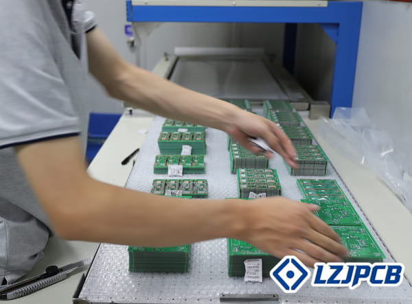
Small batch assembly requires different capabilities and processes than mass production. Based on my experience managing production at LZJPCB and working with various manufacturing partners, I’ve identified key differentiators between service providers in this specialized market.
| Company | Minimum Order | Turnaround Time | Component Sourcing | DFM Support1 | Quality Standards | Online Interface | Best For |
|---|---|---|---|---|---|---|---|
| PCBWay2 | 5 boards | 5-12 days | Parts library + procurement | Standard checks | ISO 9001, IPC Class 2 | Complete platform | General purpose prototypes, competitive pricing |
| Seeed Studio3 | 5 boards | 7-15 days | Limited parts library | Basic checks | ISO 9001, IPC Class 2 | Simple interface | Maker projects, standard designs |
| JLCPCB4 | 2 boards | 5-10 days | Basic components only | Basic automated | ISO 9001, IPC Class 2 | User friendly platform | Very simple designs, extreme cost sensitivity |
| LZJPCB5 | 5 boards | 3-10 days | Full procurement service | Comprehensive | ISO 9001, IPC Class 2-3 | Full online quoting | Complex designs, quality-critical applications |
| Elecrow | 5 boards | 7-15 days | Limited procurement | Basic checks | IPC Class 2 | Basic interface | Simple hobbyist projects |
| Advanced Circuits (China division) | 10 boards | 10-15 days | Full procurement | Advanced | IPC Class 3 | Full featured | High reliability industrial prototypes |
| ShenZhen2U | 5 boards | 7-15 days | Full procurement | Standard | ISO 9001, IPC Class 2 | Email based | Mixed technology boards |
LZJPCB5 specializes in small to medium batch production with particular strength in complex boards and quality critical applications. Our operations in China enable us to maintain competitive pricing while offering comprehensive component procurement services6—a crucial advantage given today’s challenging supply chain environment. We’ve developed specific processes for small batch production that maintain high quality standards without the setup costs typically associated with larger runs.
PCBWay2 has established itself as a popular option for small batch assembly with a user friendly online platform. They offer a good balance of price and quality for general purpose prototypes and small production runs. Their component library includes most standard parts, though specialized components may require customer supplied inventory or additional procurement time.
Seeed Studio3 caters primarily to the maker community and startups with straightforward designs. Their Fusion service offers reasonable pricing for basic assemblies, though their component library is more limited than some competitors. They’re best suited for projects using standard components and conventional design rules.
JLCPCB4 has gained popularity through extremely competitive pricing, especially for very simple boards. Their component library focuses on basic parts, making them suitable for uncomplicated designs. For complex boards or those requiring specialized components, their limitations become more apparent.
From my experience overseeing production across different facilities, I’ve observed that small batch assembly quality in China varies significantly based on several factors:
-
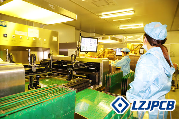
Equipment calibration and maintenance: The best small batch assemblers maintain their equipment to the same standards as their volume production lines. Lesser providers often use older, poorly maintained equipment for prototype runs, leading to higher defect rates.
-
Staff experience and training: Quality small batch production requires technicians specifically trained in prototype assembly, which involves more frequent setups and greater variation than mass production. At LZJPCB5, we have dedicated teams for small batch production rather than treating it as an afterthought.
-
Component management: Proper component storage, handling, and moisture protection are critical even for small runs. Some assemblers compromise on these standards for prototypes, leading to solderability issues and premature component failure.
-
Inspection protocols: The best small batch assemblers maintain rigorous inspection standards regardless of order size. This includes automated optical inspection (AOI), X-ray inspection for BGA and bottom terminated components, and appropriate functional testing.
-
Documentation and traceability: Quality focused assemblers maintain complete documentation even for prototype runs, including component traceability, process parameters, and inspection results.
When selecting a small batch assembler in China, communication capabilities7 significantly impact project success. Time zone differences, language barriers, and cultural differences can complicate problem resolution if not properly managed. Look for providers with:
- English speaking project managers available during your working hours
- Clear communication channels (email, messaging platforms, video conferencing)
- Documented processes for handling design changes and issues
- Willingness to provide regular production updates and photos
Geographic considerations within China also matter. The Pearl River Delta8 region (including Shenzhen and Guangzhou) offers the densest electronics manufacturing ecosystem, with excellent component availability and specialized service providers. This region typically provides the best balance of cost, quality, and speed for small batch production.
For projects requiring ongoing small batch production rather than one time prototypes, evaluate the assembler’s ability to maintain consistent quality across multiple runs. This includes document control systems, process standardization9, and component lot management—capabilities that vary widely among small batch providers.
What Is The Difference Between PCB Assembly And PCB Manufacturing?
Many new to electronics development confuse PCB assembly10 and PCB manufacturing11, leading to miscommunication with suppliers, incorrect budgeting, and unexpected project delays. This confusion creates significant problems when trying to source the right services for your project.
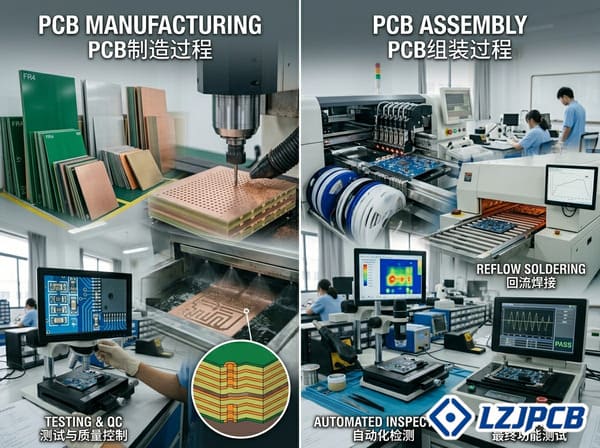
PCB manufacturing (fabrication) is the process of creating bare circuit boards from raw materials like copper clad laminates, including etching circuits, drilling holes, and applying solder mask. PCB assembly (PCBA) is the subsequent process of placing and soldering components onto these bare boards to create functional electronic assemblies.
This distinction is fundamental to understanding the electronics production process. In my role at LZJPCB, I frequently explain this difference to new clients to help them better navigate their manufacturing options. A clear understanding of these separate but related processes helps you communicate more effectively with suppliers and make better decisions about your production strategy.
Understanding the PCB Production Process: Manufacturing vs. Assembly
The PCB production process involves distinct stages that require different equipment, expertise, and quality control methods. Understanding these differences helps you select the right partners and services for your project.
| Process Stage | Definition | Key Steps | Equipment Used | Typical Timeframe | Common Issues |
|---|---|---|---|---|---|
| PCB Manufacturing (Fabrication) | Creating bare circuit boards12 | Layer preparation, lamination, drilling, plating, etching, solder mask13 application, surface finish | Laser plotters, CNC drills, plating lines, etching equipment, screen printers | 3-15 days | Etching defects, drill misalignment, delamination14 |
| PCB Assembly (PCBA) | Placing components on boards | Solder paste application, component placement15, reflow soldering16, inspection, testing | Stencil printers, pick and place machines, reflow ovens, inspection systems | 1-10 days | Solder defects, component misalignment, tombstoning17 |
| Full Turnkey Production | Complete service from design to finished product | All manufacturing and assembly steps plus component procurement18 | All manufacturing and assembly equipment plus testing systems | 2-8 weeks | Component availability, integration issues |
PCB manufacturing11 (fabrication) involves creating the bare circuit board itself. This process begins with the base material—typically FR4, a fiberglass reinforced epoxy laminate with copper foil bonded to one or both sides. For multilayer boards, multiple copper clad layers are prepared separately before being laminated together. The manufacturing process includes:
- Inner layer processing: For multilayer boards, the inner layer circuits are etched before lamination
- Lamination: Pressing the layers together under heat and pressure
- Drilling: Creating holes for vias and through hole components
- Electroless copper deposition: Adding thin copper layer to hole walls
- Electroplating: Building up copper thickness in holes and on surfaces
- Outer layer imaging and etching: Creating the outer layer circuits
- Solder mask application: Applying protective coating to prevent shorts
- Surface finish application: Adding HASL, ENIG, or other finish for solderability
- Silkscreen printing: Adding reference designators and markings
- Electrical testing: Verifying electrical continuity and isolation
- Profiling/routing: Cutting the boards to final dimensions
The PCB manufacturing11 facility contains specialized equipment for these processes, including CNC drilling machines, plating lines, etching equipment, screen printers, and automated optical inspection systems. The result is a bare circuit board with conductive pathways but no electronic components.
PCB assembly10 (PCBA) takes these bare boards and transforms them into functional electronic devices by adding components. The assembly process includes:
- Solder paste application: Applying paste to surface mount pads using a stencil
- Component placement: Positioning components precisely on the board
- Reflow soldering: Heating the assembly to melt solder paste and create connections
- Inspection: Checking for solder defects and component placement issues
- Through hole component insertion: If needed for mixed technology boards
- Wave soldering or selective soldering: For through hole components
- Final inspection: Verifying overall assembly quality
- Functional testing: Confirming the board works as intended
- Conformal coating: Optional protective coating for harsh environments
- Packaging: Preparing boards for shipping
Assembly facilities contain different equipment, including solder paste printers, pick and place machines, reflow ovens, wave soldering19 systems, and various inspection technologies. The skill sets required also differ, with assembly technicians needing expertise in soldering techniques, component handling, and electronics testing.
From a business perspective, many companies specialize in either PCB manufacturing11 or assembly, though full service providers like LZJPCB offer both services. This integration provides several advantages:
- Streamlined communication: Working with one provider eliminates handoff issues
- Design for manufacturability: Integrated providers can optimize designs for both processes
- Reduced logistics costs: No shipping between separate manufacturers and assemblers
- Faster turnaround: Eliminating transportation and communication delays
- Simplified accountability: One provider responsible for the entire process
When comparing quotes, be careful to understand exactly what services are included. Manufacturing only quotes cover just the bare board production, while assembly quotes might or might not include component procurement18. "Turnkey" services typically include both manufacturing and assembly plus component procurement18, but always verify the specific scope.
Component procurement represents another significant distinction. In a "turnkey" arrangement, the service provider handles all component sourcing. With "consigned" or "kitted" assembly, you provide the components yourself. Each approach has advantages:
Turnkey advantages:
- Simplified process with single point responsibility
- Leverage of supplier’s purchasing power and component relationships
- Reduced logistics management on your end
- Often faster overall timeline
Consigned/kitted advantages:
- Direct control over component selection and sourcing
- Potentially lower markup on component costs
- Ability to use existing component inventory
- Better control over component quality for critical parts
For new product development, I typically recommend a turnkey approach for prototypes and initial production to simplify the process, then evaluating whether to transition to a consigned model for larger production volumes once the design is stable. This approach maximizes development speed while maintaining cost control for production.
What Are The 7 Types Of PCB Testing Methods?
Inadequate testing can allow defective boards20 to reach the field, resulting in costly recalls, warranty claims, and damaged reputation. Many companies struggle to determine which testing methods are necessary for their specific products, either overspending on unnecessary tests or risking failures through insufficient testing.
The seven primary PCB testing methods are: 1) Automated Optical Inspection (AOI) for visual defects, 2) In Circuit Testing (ICT) for component values and connections, 3) Flying Probe Testing for electrical verification, 4) Functional Testing for operational verification, 5) X-ray Inspection for hidden joints, 6) Burn in Testing for reliability screening, and 7) Environmental Testing for operation under stress conditions.
PCB testing21 is critical for ensuring product quality and reliability. At LZJPCB, we implement comprehensive testing strategies22 tailored to each product’s requirements and application. The appropriate testing combination depends on factors including production volume23, board complexity24, application criticality25, and budget constraints. Understanding these methods helps you make informed decisions about your testing requirements.
Comprehensive PCB Testing Methodologies
Each testing method serves specific purposes and has distinct advantages and limitations. Based on my experience implementing testing protocols for various product categories, I can provide insight into selecting the most effective combination for your specific needs.
| Testing Method | What It Tests | When To Use | Advantages | Limitations | Typical Cost |
|---|---|---|---|---|---|
| Automated Optical Inspection (AOI)26 | Component placement, polarity, solder quality | All production | Fast, non contact, high defect detection27 | Can’t detect internal or functional defects | Low to moderate |
| In Circuit Testing (ICT)28 | Component values, connections, basic function | Medium to high volume | Comprehensive electrical testing, high fault coverage | Requires expensive fixtures, design for test | Moderate to high |
| Flying Probe Testing29 | Electrical connections, component presence | Prototypes, low volume | No fixtures required, flexible | Slower than ICT, less comprehensive | Moderate |
| Functional Testing30 | Operation as intended | All production | Verifies actual functionality | Custom development required, may miss some defects | Moderate to high |
| X-ray Inspection31 | Hidden solder joints, BGA connections | Boards with BGAs, QFNs | Can see defects invisible to other methods | Expensive, slower, specialized operation | High |
| Burn in Testing32 | Early life failures | High reliability products | Identifies weak components | Time consuming, requires environment control | Moderate to high |
| Environmental Testing33 | Performance under stress | Products for harsh environments | Verifies operation under real conditions | Destructive testing, expensive equipment | High |
Automated Optical Inspection (AOI)26 is typically the first line of defense in PCB testing21. Modern AOI systems use high resolution cameras and sophisticated algorithms to detect visual defects including missing components, incorrect component placement, polarity errors, and solder defects34. The advantages of AOI include fast inspection speed, no physical contact with the board, and the ability to catch defects early in the production process. However, AOI can’t detect internal defects or functional issues.
At LZJPCB, we use AOI for 100% of our assembled boards. The system compares each board against the design data and automatically flags potential defects for human verification. We’ve found that combining automated and human inspection provides the highest detection rates for visual defects.
In Circuit Testing (ICT)28 uses a "bed of nails" fixture—a custom designed array of spring loaded pins that contact test points on the PCB. This allows detailed electrical testing of individual components and connections without powering up the entire circuit. ICT can detect component value errors, shorts, opens, and basic functional issues. The main advantage is comprehensive coverage, but the custom fixtures35 are expensive and require specific design considerations (test points) on the PCB.
ICT makes economic sense for medium to high volume production, typically runs of 300+ identical boards where the fixture cost can be amortized. For medical and automotive applications, we often recommend ICT despite the higher setup costs due to its superior test coverage36.
Flying Probe Testing29 provides similar electrical testing to ICT but uses mobile probes that move to contact various points on the board rather than a fixed fixture. This eliminates the need for expensive custom fixtures35, making it ideal for prototypes and low volume production. The tradeoff is significantly slower test speed compared to ICT. Flying probe testing typically costs $200-500 per board design but requires no additional setup costs for new designs.
We recommend flying probe testing for all first article boards and low volume production runs, especially for complex designs where manual inspection might miss connection issues.
Functional Testing30 verifies that the assembled PCB operates as intended in its actual application. This involves powering the board and running it through typical operations while monitoring outputs and behavior. The test equipment ranges from simple power supplies and multimeters to sophisticated automated test systems that simulate the product’s operating environment. The advantage of functional testing is that it verifies actual operation rather than just individual components, but it requires custom development for each product.
For critical applications, we typically develop functional test fixtures that verify key performance parameters. These might include communication protocols, sensor readings, power consumption profiles, or timing specifications depending on the product function.
X-ray Inspection31 has become increasingly important as components like BGAs (Ball Grid Array) and QFNs (Quad Flat No leads) with hidden connections have become common. X-ray systems allow inspection of solder joints that are physically hidden from view. This technology is particularly valuable for high density boards where visual inspection cannot confirm proper connections. The limitations include high equipment cost and specialized operator training requirements.
We recommend X-ray inspection for all boards with BGA components, particularly in early production runs or when establishing new assembly processes. For ongoing production, we typically use statistical X-ray inspection based on defect rates and criticality.
Burn in Testing32 identifies early life failures by operating boards under stress (typically elevated temperature) for an extended period before shipment. This accelerates the "infant mortality" period where weak components tend to fail. Burn in is particularly important for high reliability applications where field failures would be extremely costly or dangerous. The main disadvantage is the additional production time and specialized environmental equipment required.
For medical devices and industrial control systems, we typically recommend 24-48 hour burn in testing with power cycling to stress the components and identify any marginal assemblies before they reach the field.
Environmental Testing33 subjects boards to conditions they might encounter during use, including temperature extremes, humidity, vibration, and shock. This testing verifies that the product will function reliably in its intended environment. Environmental testing often requires specialized chambers and equipment and may be destructive in nature. It’s typically performed on samples rather than 100% of production.
For products designed for harsh environments—such as automotive, outdoor, or industrial applications—we recommend environmental sample testing for each significant production batch. This might include temperature cycling, humidity exposure, or vibration testing depending on the expected operating conditions.
Developing an effective testing strategy requires balancing detection capability, cost, and production impact. For most products, we recommend a combination of testing methods:
- AOI for 100% of boards to catch visual and surface defects
- ICT or Flying Probe (depending on volume) for electrical verification
- Functional testing for operational confirmation
- Selective X-ray inspection based on component types
- Environmental testing based on the application environment
The testing investment should be proportional to the consequences of failure. Medical devices, automotive systems, industrial controls, and aerospace applications warrant more comprehensive testing than consumer electronics with limited lifespan expectations or non critical functions.
Conclusion
Choosing a reliable PCB assembly partner requires evaluating certifications, manufacturing capabilities, quality control processes, and communication systems. For small batch production in China, companies like LZJPCB offer specialized services with appropriate testing methods. Understanding the distinction between PCB manufacturing and assembly helps you source services effectively, while implementing appropriate testing strategies ensures product quality and reliability in your specific application.
-
Explore the concept of Design for Manufacturability (DFM) support and its significance in PCB assembly. ↩
-
Learn why PCBWay is favored for small batch assembly and how they balance price and quality. ↩ ↩
-
Find out how Seeed Studio supports makers and startups with their PCB assembly services. ↩ ↩
-
Explore JLCPCB’s competitive pricing and suitability for simple designs in PCB assembly. ↩ ↩
-
Discover LZJPCB’s unique offerings and how they can cater to your specific PCB assembly needs. ↩ ↩ ↩
-
Understand the importance of component procurement services in ensuring timely and efficient PCB assembly. ↩
-
Understand the role of effective communication in ensuring successful PCB assembly projects. ↩
-
Discover why the Pearl River Delta is a key region for electronics manufacturing and PCB assembly. ↩
-
Learn about the benefits of process standardization in maintaining quality across PCB assembly runs. ↩
-
Exploring PCB assembly helps you grasp how electronic components are integrated into circuit boards, essential for product development. ↩ ↩
-
Understanding PCB manufacturing is crucial for anyone involved in electronics, as it lays the foundation for creating circuit boards. ↩ ↩ ↩ ↩
-
Circuit boards are the backbone of electronic devices; learning about them enhances your knowledge of electronics. ↩
-
The solder mask is vital for preventing shorts; understanding it can improve your PCB design and manufacturing process. ↩
-
Delamination can lead to board failure; understanding its causes can help you avoid costly manufacturing errors. ↩
-
Effective component placement is key to successful assembly; exploring best practices can improve your design outcomes. ↩
-
Reflow soldering is essential for creating reliable electronic connections; learning about it can enhance your assembly knowledge. ↩
-
Tombstoning is a common defect in assembly; learning how to prevent it can enhance your production quality. ↩
-
Component procurement is a key factor in assembly efficiency; knowing its nuances can optimize your production strategy. ↩ ↩ ↩
-
Wave soldering is a common technique for through-hole components; understanding it can enhance your assembly process. ↩
-
Explore the potential consequences of defective boards reaching the market. ↩
-
Understand the significance of PCB testing in preventing costly recalls and ensuring reliability. ↩ ↩
-
Explore various testing strategies to enhance PCB quality and reliability. ↩
-
Discover how production volume influences the choice of PCB testing strategies. ↩
-
Learn how the complexity of a PCB design affects testing requirements and methods. ↩
-
Understand the importance of application criticality in determining testing strategies. ↩
-
Explore AOI to understand how it enhances defect detection and improves PCB quality. ↩ ↩
-
Learn about best practices to improve defect detection rates in PCB production. ↩
-
Learn about ICT’s comprehensive electrical testing and its importance in high-volume production. ↩ ↩
-
Discover the flexibility and advantages of Flying Probe Testing for low volume and prototype boards. ↩ ↩
-
Understand how Functional Testing verifies actual operation and performance of PCBs. ↩ ↩
-
Find out how X-ray Inspection reveals hidden defects in high-density PCB designs. ↩ ↩
-
Explore how Burn in Testing identifies early life failures in critical applications. ↩ ↩
-
Learn about Environmental Testing and its role in ensuring reliability under stress conditions. ↩ ↩
-
Learn about methods to identify solder defects and ensure PCB quality. ↩
-
Understand the role of custom fixtures in enhancing the effectiveness of ICT. ↩ ↩
-
Discover the significance of test coverage in ensuring comprehensive PCB evaluations. ↩