Skip to content
 Meeting production deadlines is critical in electronics development, but unpredictable PCB assembly timeframes can derail your entire project schedule. Stakeholders expect consistent delivery dates, yet many engineers find themselves unable to provide reliable estimates for this crucial manufacturing step.
PCB assembly typically takes 1-3 days for simple prototypes with in stock components, 5-10 days for standard small batch production, and 2-4 weeks for complex or volume production runs. Timing varies significantly based on design complexity, component availability, testing requirements, and production volume.
Understanding realistic PCB assembly timeframes is essential for project planning and meeting market windows. As someone who’s managed thousands of assembly projects at LZJPCB, I’ve seen how timing varies dramatically based on multiple factors. The best electronics teams build accurate assembly timing into their development schedules, accounting for the variables that can extend or compress production timeframes.
What Is The Standard For PCB Assembly?
When planning electronics manufacturing, vague industry standards can lead to misaligned expectations and costly delays. Many engineers struggle to communicate realistic timelines to management because assembly standards vary widely across the industry.
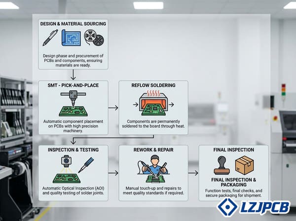
The standard process for PCB assembly includes component procurement (1-4 weeks), solder paste application (minutes to hours), component placement using pick and place equipment (hours to days), soldering via reflow or wave processes (hours), inspection (hours to days), and testing (hours to days).
After years in PCB manufacturing, I’ve found that understanding the complete assembly process helps set realistic expectations. While quick turn services advertise rapid turnaround times, these often apply only to specific scenarios with all components in stock and designs ready for production. Let me explain what actually happens during the assembly process to give you a clearer picture of standard timeframes.
Understanding PCB Assembly Standards and Processes
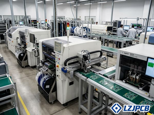
Standard PCB assembly1 involves multiple steps that must be completed in sequence, each with its own timeline considerations. I’ve seen many projects delayed because planners didn’t account for the full process or understand how different factors affect each stage.
| Assembly Stage | Standard Timeframe | Key Variables | Potential Delays |
|---|---|---|---|
| Component Procurement | 1-4 weeks | Component availability, order volume | Semiconductor shortages, obsolete parts, minimum order quantities |
| Material Preparation | 1-3 days | Board complexity, stencil fabrication | Custom stencil requirements, special handling needs |
| Solder Paste Application | Minutes to hours | Board size, number of boards | Stencil alignment issues, paste consistency problems |
| Component Placement | Hours to days | Component count, component types | Fine pitch components, unusual packages, manual placement needs |
| Reflow/Wave Soldering | Hours | Board size, assembly technology | Profile development for complex boards, mixed technology requirements |
| Inspection | Hours to days | Quality standards, inspection method | Defect resolution, additional inspection requirements |
| Testing | Hours to days | Test complexity, test coverage | Test fixture development, troubleshooting failed tests |
| Rework (if needed) | Hours to days | Defect types, board accessibility | Component availability for replacement, complex rework needs |
| Conformal Coating/Final Finishing | Hours to days | Coating requirements, curing time | Additional masking requirements, multi stage processes |
Component procurement remains the most variable and often longest part of the assembly timeline. In today’s challenging supply chain environment2, even common components can have extended lead times. At LZJPCB, we maintain inventory of frequently used components to minimize this variable, but custom or specialized parts often must be ordered specifically for each project.
The material preparation stage includes programming pick and place machines, creating solder paste stencils, and preparing the production environment. For repeat orders, this stage is significantly faster as the setup information is already established. First time orders require additional preparation time, particularly for complex designs with many unique components.
The actual assembly process—applying solder paste, placing components, and soldering—is relatively standardized and predictable. Modern pick and place machines can place thousands of components per hour, making this stage surprisingly fast even for complex boards. However, boards with unusual components or requiring manual placement will take longer.
Inspection and testing timeframes vary dramatically based on the requirements. Simple visual inspection might take minutes per board, while comprehensive automated optical inspection (AOI), X-ray inspection for hidden joints, and functional testing can extend to hours per board for complex designs. The standards applied also matter—military, aerospace, or medical products typically undergo more rigorous inspection than consumer electronics.
Rework, when necessary, can significantly extend assembly time. In high reliability applications, each rework action must be documented, inspected, and sometimes re tested, adding hours or days to the process. The industry standard is to minimize rework through proper design and process control, but some level of rework is common, especially for prototypes and first production runs.
Industry standards for assembly timing also vary by service level. "Standard" service typically means 5-10 business days, "expedited" service 3-5 business days, and "super rush" service 1-2 business days. However, these timeframes generally assume all components are available and the design is ready for production without modifications.
The assembly standard also includes documentation requirements3 that vary by industry. Consumer electronics might need basic production records, while medical devices require comprehensive documentation of every process step, material lot, and test result. These documentation standards significantly impact the overall timeline, especially for regulated industries.
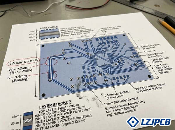
What Is The 3W Rule In PCB?
Many designers create PCB layouts that look perfect in CAD but cause serious manufacturing problems. Without understanding fundamental design rules like the 3W rule4, you risk costly redesigns, manufacturing defects5, and project delays.
The 3W rule in PCB design states that the spacing between copper features should be at least three times the width of the copper pour being used. For example, if your copper pour is 0.5mm wide, the spacing to adjacent copper should be at least 1.5mm to ensure reliable manufacturing and prevent potential shorts.
Design rules like the 3W guideline directly impact manufacturing time and reliability. At LZJPCB, we routinely perform design for manufacturing (DFM) reviews6 that identify spacing issues before production. I’ve seen countless cases where inadequate spacing led to manufacturing defects5 that could have been easily prevented at the design stage.
The 3W Rule and Other Key PCB Design Standards
The 3W rule4 is just one of many design guidelines that ensure manufacturability7 and reliability. Understanding these standards helps create designs that can be assembled efficiently and function reliably over time.
| Design Rule | Description | Standard Value | Impact on Manufacturing |
|---|---|---|---|
| 3W Rule | Spacing between copper pours | 3x copper width | Prevents shorts during etching, improves yield |
| Trace Width | Minimum width of copper traces | 4-8 mil (0.1-0.2mm) | Affects current capacity and manufacturing yield |
| Via Size | Diameter of plated holes | 0.3-0.5mm | Impacts drilling precision and plating quality |
| Component Spacing | Distance between components | 0.5-1.0mm | Affects assembly equipment access and rework capability |
| Edge Clearance | Distance from board edge to components | 5mm recommended | Prevents damage during depanelization and handling |
| Thermal Relief | Connection between planes and vias/pads | 4 spokes standard | Prevents soldering issues from heat sinking |
| Silkscreen Width | Minimum line width for text/symbols | 5-6 mil (0.12-0.15mm) | Ensures readability and manufacturing quality |
| Solder Mask Bridge | Minimum width between exposed pads | 4-5 mil (0.1-0.12mm) | Prevents solder bridges and shorts |
The 3W rule4 specifically addresses the relationship between copper width and spacing in power planes, ground planes, and other large copper areas. When copper is etched during PCB manufacturing, the etching process works laterally as well as vertically. Insufficient spacing can lead to under etching where copper that should be removed remains, potentially causing shorts between supposedly isolated traces or planes.
From my manufacturing experience, I can tell you that boards designed with proper spacing according to the 3W rule4 have significantly higher first pass yield rates. This directly translates to faster manufacturing time and lower costs. When spacing is too tight, the manufacturing process must be slowed down and carefully monitored, extending production time.
Component spacing standards are equally important for assembly efficiency. Modern pick and place machines can place components very close together, but inadequate spacing creates problems during soldering and inspection. I recommend maintaining at least 0.5mm between small components and 1.0mm or more between larger components to allow for efficient assembly and rework if needed.
Edge clearance requirements often surprise new designers. Components placed too close to the board edge risk damage during depanelization (when individual boards are separated from a panel) and during normal handling. Most manufacturers recommend at least 5mm clearance from the board edge to any component, though this can be reduced to 3mm in space constrained designs if special handling procedures are implemented.
Thermal relief connections are another critical design standard that affects assembly time. When pads or vias connect directly to large copper planes without thermal relief8, they can be extremely difficult to solder properly because the plane acts as a heat sink. Standard practice is to use "spoke" connections that provide electrical connectivity while thermally isolating the pad enough for efficient soldering.
Solder mask design standards are particularly important for fine pitch components. The solder mask bridge9 (the mask material between exposed pads) must be wide enough to actually form during manufacturing. If specified too narrow, the mask may not properly separate pads, leading to solder bridges during assembly.
Adhering to these design standards significantly improves manufacturability7, reduces assembly time, and increases reliability. At LZJPCB, designs that follow these guidelines typically move through production 30-40% faster than designs requiring special handling or modifications. For quick turn projects, design rule compliance is especially critical, as non standard designs often cannot be accommodated in expedited timeframes.
Where Can I Find Reputable Companies Offering Quick Turn PCB Assembly Services?
When facing tight deadlines, finding reliable quick turn assembly partners can be overwhelming. Many services promise fast turnaround but deliver inconsistent quality or miss deadlines, leaving your project in jeopardy at the most critical moment.
Reputable quick turn PCB assembly providers include established manufacturers like LZJPCB, Sierra Circuits, and Advanced Circuits, online services like PCBWay and JLCPCB, and regional specialists in electronics manufacturing hubs. The best choice depends on your volume needs, component requirements, quality standards, and geographic location.
Finding the right quick turn assembly partner requires considering multiple factors beyond just the advertised turnaround time. Through my years in the industry, I’ve developed relationships with various manufacturers and can provide insight into what makes certain providers more reliable than others for expedited services.
Evaluating Quick Turn PCB Assembly Service Providers
Selecting the right quick turn assembly partner involves evaluating several key capabilities and service characteristics. Based on my experience managing urgent projects, these factors most strongly predict successful outcomes for time critical assemblies.
| Provider Type | Typical Turnaround | Strengths | Limitations | Best For |
|---|---|---|---|---|
| Full Service Manufacturers (LZJPCB10, Sierra Circuits11) | 1-10 days | Component sourcing, DFM support, comprehensive testing | Higher costs, minimum order values | Complex designs, full turnkey needs |
| Online Service Platforms (PCBWay12, JLCPCB13) | 1-7 days | Streamlined ordering, transparent pricing, basic assembly | Limited component selection, basic support | Simple designs, standard components |
| Regional Specialists | 1-5 days | Local support, flexible processes, rush capabilities | Geographic limitations, variable capacity | Collaborative projects, unique requirements |
| High Volume Asian Manufacturers | 3-14 days | Cost efficiency, scale capabilities | Communication challenges, longer shipping | Price sensitive projects with flexible timing |
| Ultra Fast Specialists (Screaming Circuits) | 24-72 hours | Extremely fast turnaround, emergency service | Premium pricing, limited capacity | Critical deadlines, emergency replacements |
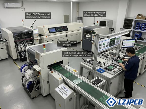
Full service manufacturers like LZJPCB offer comprehensive quick turn capabilities for more complex projects. Our advantage is the ability to handle the entire process from component procurement through final testing, with engineering support throughout. We maintain inventory of commonly used components specifically to support quick turn projects and have dedicated production lines for expedited orders. The limitation is that these services typically come at a premium price compared to standard lead times.
Online service platforms have revolutionized quick turn assembly access for simple to moderate complexity boards. Services like PCBWay12 and JLCPCB13 offer user friendly interfaces for uploading designs, selecting components from their inventory, and choosing service levels. These platforms are excellent for straightforward designs using standard components, but may struggle with highly specialized requirements or complex assemblies.
Regional specialists often excel at quick turn services within their geographic area. In North America, companies like Advanced Circuits14 and Sunstone Circuits have built reputations for reliable quick turn capability. In Europe, Eurocircuits and Beta LAYOUT offer similar services. These regional providers typically offer excellent communication and can accommodate special requirements, but may have higher costs than Asian manufacturers.
Traditional high volume Asian manufacturers15 have increasingly developed specialized quick turn capabilities to complement their mass production services. While these providers may not match the 24-48 hour turnaround of dedicated quick turn specialists, they often offer excellent value for projects with 5-10 day timeframes. The main challenges involve communication across time zones and international shipping times.
For the most critical deadlines, ultra fast specialists16 like Screaming Circuits in the US focus exclusively on rapid turnaround, sometimes offering same day service for emergency needs. These services come at a significant premium but can be invaluable when facing immovable deadlines or needing emergency replacements for failed units.
When evaluating quick turn providers, look beyond just the advertised turnaround times to understand the complete capability:
-
Component sourcing approach: Some quick turn services require you to provide all components, while others keep inventory of common parts or offer procurement services. At LZJPCB, we maintain inventory of thousands of common components specifically for quick turn projects.
-
Design for Manufacturing (DFM) review17: Quality quick turn providers perform expedited but thorough DFM reviews to catch issues before production. This prevents delays from discovering problems mid production.
-
Testing capabilities: Understand what level of testing is included with quick turn services. Some providers offer only basic continuity testing, while others can provide comprehensive functional testing even on expedited timelines.
-
Actual delivered quality: Request sample photos of previously assembled boards or, if possible, actual samples. This provides tangible evidence of the quality you can expect.
-
Communication systems: Effective quick turn assembly requires excellent communication. Look for providers with online tracking systems, responsive project managers, and clear escalation paths if issues arise.
-
Geographic considerations: For extremely time sensitive projects, local providers may offer advantages in both communication and shipping time, even if their production costs are higher.
-
Scalability path: Consider whether the quick turn provider can also support transition to higher volume if your prototype is successful. This can simplify the path to production.
At LZJPCB, we’ve developed specialized workflows for handling quick turn projects without compromising quality. This includes dedicated procurement specialists for component sourcing, expedited DFM reviews, and reserved capacity on our production lines specifically for urgent projects. For clients with recurring quick turn needs, we also maintain component inventory and process documentation to further streamline future orders.
Conclusion
PCB assembly timing depends on design complexity, component availability, volume, and quality requirements. Standard assembly follows established processes that typically take 1-3 weeks, though quick turn services can deliver in days. Following design rules like the 3W standard helps ensure efficient manufacturing and reliable performance of your electronic assemblies.
-
Explore this link to understand the best practices that can enhance your PCB assembly process and efficiency. ↩
-
Discover how the current supply chain challenges impact PCB assembly timelines and strategies to mitigate risks. ↩
-
Explore the essential documentation requirements to ensure compliance and efficiency in your assembly process. ↩
-
Understanding the 3W rule is crucial for preventing manufacturing defects and ensuring reliable PCB designs. ↩ ↩ ↩ ↩
-
Learning about manufacturing defects can help designers avoid costly mistakes and improve design quality. ↩ ↩
-
DFM reviews help identify potential design issues early, saving time and costs in the manufacturing process. ↩
-
Improving manufacturability leads to faster production times and reduced costs, crucial for successful PCB projects. ↩ ↩
-
Thermal relief is essential for effective soldering and preventing heat related issues in PCB assembly. ↩
-
A proper solder mask bridge prevents solder bridges, ensuring reliable connections in fine pitch components. ↩
-
Learn about LZJPCB’s offerings for quick turn pcb assembly and how they can meet your urgent project needs. ↩
-
Learn about Sierra Circuits’ strengths in quick turn assembly and how they can meet your urgent project needs. ↩
-
Explore PCBWay’s user friendly platform and services that streamline the quick turn assembly process. ↩ ↩
-
Check out JLCPCB’s offerings for quick turn assembly and how they cater to simple designs efficiently. ↩ ↩
-
Find out why Advanced Circuits is a trusted choice for quick turn PCB assembly with their local support and expertise. ↩
-
Learn about the pros and cons of high volume Asian manufacturers in the context of quick turn PCB assembly. ↩
-
Discover how ultra fast specialists can meet critical deadlines with rapid turnaround services for PCB assembly. ↩
-
Explore the significance of DFM reviews in ensuring quality and efficiency in quick turn PCB assembly. ↩