Skip to content
 Electronic engineers facing complex PCB design challenges often wonder if AI tools like ChatGPT could streamline their workflow. With mounting pressure to reduce design time and growing PCB complexity, the promise of AI assistance is tempting, yet many are unsure of its actual capabilities and limitations.
ChatGPT cannot directly create PCB designs or generate manufacturing files like Gerbers. It lacks integration with PCB design software and cannot manipulate CAD files. However, it can provide design guidance, suggest component placement strategies, calculate electrical parameters, troubleshoot design issues, and help optimize layouts through text based recommendations.
In my work at LZJPCB, I’ve seen firsthand how the PCB design process combines technical knowledge with creative problem solving. While AI tools like ChatGPT offer promising support for certain aspects of PCB design, understanding their true capabilities and limitations is essential for engineers looking to incorporate these tools into their workflow. Let me share some practical insights on how ChatGPT can and cannot help with your PCB design projects.
How Hard Is It To Learn PCB Design?
Many engineers and electronics enthusiasts feel intimidated by PCB design1, seeing complex multilayer boards and wondering if they can ever master such a specialized skill. This hesitation often delays projects and limits innovation as people rely on pre made modules rather than custom designs.
Learning basic PCB design takes 2-3 months of dedicated practice, while mastering advanced techniques requires 1-3 years of professional experience. The learning curve includes understanding schematic capture (easiest), component selection, layout fundamentals, and advanced topics like signal integrity and high speed design (most challenging).
PCB design1 combines electrical engineering principles with specialized software skills and manufacturing knowledge. I’ve trained many new PCB designers at LZJPCB, and I’ve observed consistent patterns in the learning journey. While the basics can be grasped relatively quickly, developing true expertise requires time and deliberate practice across increasingly complex projects.
The PCB Design Learning Curve: From Beginner to Expert
Learning PCB design1 involves multiple skill areas that build upon each other. Based on my experience training designers and working with clients at various skill levels, I’ve developed a framework for understanding this learning progression.
| Skill Level | Time Investment | Key Skills | Software Proficiency | Common Challenges | Project Complexity |
|---|---|---|---|---|---|
| Beginner | 1-2 months | Basic schematic capture2, simple component placement, single/double layer routing | Basic software navigation, simple commands | DRC errors, manufacturing constraints, footprint selection | Simple breakout boards, Arduino shields, basic sensor circuits |
| Intermediate | 3-6 months | Multi layer routing, power planes, DFM considerations3, BOM management | Custom component creation, keyboard shortcuts, design rule setup | Signal integrity basics, thermal management4, layout optimization | Multi layer boards, moderate component density, basic mixed signal |
| Advanced | 1-2 years | Impedance control, high speed design5, power integrity, flex/rigid flex design | Advanced automation, scripting, library management | EMI/EMC compliance, advanced stackup planning, controlled impedance | High density boards, RF designs, high speed digital |
| Expert | 3+ years | Complex system architecture, cutting edge technologies, advanced DFM/DFA | Custom plugins, API integration, design automation | Leading edge processes, advanced manufacturing techniques | Military/aerospace, medical devices, high reliability systems |
The initial learning phase focuses on basic schematic capture2 and simple board layouts. This stage typically takes 1-2 months of consistent practice and involves learning software basics and fundamental concepts like:
- Creating and reading schematics
- Understanding basic electrical components and their symbols
- Learning footprint selection and component placement
- Basic routing techniques for single or double layer boards
- Setting up design rules and constraints
Most beginners find schematic capture2 relatively straightforward if they have basic electronics knowledge. The more significant challenge comes with translating schematics into physical layouts. Common beginner mistakes include insufficient clearances, improper pad sizes, and not considering manufacturing limitations.
I recommend starting with simple projects like LED circuits, basic sensor interfaces, or Arduino shields. These projects provide practical experience without overwhelming complexity. Open source platforms like Arduino offer excellent starting points because they provide working examples and community support.
The intermediate stage typically requires 3-6 months of regular practice and involves more complex designs with:
- Multi layer board layouts
- Proper use of ground and power planes
- More advanced component packages (QFN, BGA)
- Design for manufacturing (DFM) considerations
- Basic signal integrity6 concepts
At this stage, designers start creating more complex circuits with microcontrollers, multiple interfaces, and mixed analog/digital designs. The challenges shift from simply making connections to optimizing layouts for performance and reliability.
A common hurdle at the intermediate level is managing component libraries effectively. Creating and maintaining accurate footprints becomes crucial as designs grow more complex. Many intermediate designers struggle with the transition from "making it work" to "making it manufacturable and reliable."
The advanced stage typically requires 1-2 years of professional experience and involves:
- High speed digital design techniques
- Proper stackup planning for signal integrity6
- Power integrity analysis and optimization
- Impedance control and transmission line theory
- EMI/EMC considerations
At this level, designers work on complex multilayer boards with high speed interfaces like USB, Ethernet, or DDR memory. The challenges become increasingly technical, requiring deeper understanding of electrical engineering principles beyond just the mechanical aspects of layout.
Advanced designers must understand concepts like controlled impedance, return path analysis, and proper decoupling strategies. They also need to consider thermal management4, especially for high power components or densely packed designs.
Expert level PCB design1 typically requires 3+ years of professional experience with complex projects and includes:
- System architecture optimization
- Advanced manufacturing technologies (HDI, microvia, etc.)
- Design for specialized environments (military, medical, aerospace)
- Custom design automation and methodology development
- Leading cross functional teams through complex design processes
Experts work on the most demanding projects high reliability systems, ultra high speed designs, and cutting edge technologies. They often develop proprietary design methodologies and contribute to advancing the field.
The learning resources available today have significantly reduced the time required to reach proficiency. When I started in PCB design1, information was limited to expensive textbooks and in person training. Today’s designers benefit from:
- Online tutorial videos and courses
- Interactive software tutorials
- Community forums and discussion groups
- Open source design examples
- Manufacturer design guidelines and resources
Software choice significantly impacts the learning curve. Entry level tools like EasyEDA or KiCad7 offer gentler learning curves but may have limitations for advanced work. Professional tools like Altium Designer8, Cadence Allegro, or Mentor PADS provide more capabilities but have steeper learning curves.
At LZJPCB, we’ve observed that designers from different backgrounds approach PCB design1 differently:
- Electrical engineers typically grasp circuit concepts quickly but may struggle with the mechanical aspects and manufacturing considerations
- Mechanical engineers excel at component placement and board outlines but may need more time to understand signal integrity6 concepts
- Software engineers often adapt quickly to the software interface but need more time with electrical concepts and component selection9
- Self taught hobbyists sometimes develop creative solutions but may miss formal design principles that ensure reliability
The biggest challenge for most learners isn’t the software itself but developing the "PCB mindset10"—thinking simultaneously about electrical performance, physical constraints, thermal considerations, manufacturing limitations, and long term reliability. This multidisciplinary thinking takes time to develop through varied project experience.
For those just starting, I recommend focusing on understanding rather than memorizing. Learning why certain design practices exist (rather than just following rules) builds a foundation that transfers across different software tools and project types. Start with simple projects, analyze existing designs, and gradually increase complexity as your confidence grows.
What Is The Salary Of A PCB Designer?
When considering a career in PCB design or hiring design talent, the wide variation in reported salaries can be confusing. Without clear salary benchmarks, professionals may undervalue their skills or companies may struggle to make competitive offers in this specialized field.
PCB designer salaries range from $45,000-$60,000 for entry level positions, $60,000-$85,000 for mid level designers, and $85,000-$120,000+ for senior designers with specialized expertise. Factors affecting compensation include location, industry specialization, software proficiency, and additional skills like signal integrity analysis or component engineering.

As someone who has both hired PCB designers and advised professionals in the field, I’ve gained insight into the compensation landscape across different regions and specializations. The PCB design profession offers solid career prospects with compensation that reflects the specialized technical knowledge required. Let me share a more detailed breakdown of the factors that influence PCB designer salaries11.
PCB Designer Compensation: Factors and Market Trends
PCB designer salaries11 vary significantly based on multiple factors including experience level, geographic location12, industry specialization13, and technical expertise. Based on my industry experience and market research, I’ve compiled this comprehensive analysis of compensation patterns.
| Experience Level | US Salary Range | European Salary Range | Asian Salary Range | Key Skills Expected | Industries Paying Premium |
|---|---|---|---|---|---|
| Entry Level (0-2 years) | $45,000-$60,000 | €35,000-€50,000 | $12,000-$30,000 | Schematic capture, basic layout, 2-4 layer boards | Consumer electronics, general manufacturing |
| Mid Level (3-7 years) | $60,000-$85,000 | €50,000-€70,000 | $30,000-$50,000 | Multi layer designs, DFM expertise, complex component packages | Telecommunications, industrial, automotive |
| Senior (8-15 years) | $85,000-$120,000 | €70,000-€90,000 | $50,000-$80,000 | High speed design, signal integrity, team leadership | Defense, medical, aerospace |
| Expert/Specialist (15+ years) | $120,000-$150,000+ | €90,000-€120,000+ | $80,000-$100,000+ | System architecture, cutting edge technologies, consultative expertise | Aerospace, defense, high end computing |
Geographic location significantly impacts PCB designer salaries11. Within the United States, technology hubs command premium compensation:
- Silicon Valley/San Francisco: 25-40% above national average
- Boston/Northeast tech corridor: 15-25% above national average
- Austin, Texas: 5-15% above national average
- Research Triangle (NC): Near national average
- Midwest/Southern regions: 5-15% below national average
European salaries typically run 10-20% lower than their US counterparts for equivalent positions, though this gap narrows at higher experience levels. Within Europe, Switzerland, Germany, and the Netherlands typically offer the highest compensation, while Eastern European countries offer significantly lower salaries but are growing rapidly as design centers.
Asian markets show the widest variation, with Japan and Singapore offering salaries closest to Western levels, while China, Malaysia, and the Philippines offer lower compensation but provide extensive growth opportunities. Many PCB designers in these regions advance quickly to team leadership roles due to the rapid expansion of electronics manufacturing in these areas.
Industry specialization creates significant salary differentiation. PCB designers focusing on these high demand specialties often command 15-30% salary premiums:
- Defense/aerospace: Requires security clearances, compliance knowledge, and high reliability design expertise
- Medical devices: Demands thorough documentation, regulatory compliance, and exceptional attention to detail
- High performance computing: Requires advanced signal integrity skills and cutting edge interface design
- Telecommunications infrastructure: Needs RF expertise, high speed digital skills, and large complex system experience
- Automotive safety systems: Requires functional safety certification knowledge and high reliability design
Software proficiency impacts earning potential as well. Designers with expertise in premium tools like Altium Designer, Cadence Allegro, or Mentor Graphics typically earn 10-15% more than those working exclusively with entry level tools. The highest paid specialists often have proficiency across multiple platforms and can easily adapt to client specific requirements.
Beyond basic layout skills, several technical specializations can significantly boost compensation:
- Signal integrity analysis: 15-25% premium
- RF/microwave design: 20-30% premium
- Flex and rigid flex design: 10-20% premium
- HDI (High Density Interconnect) expertise: 15-25% premium
- FPGA specific design experience: 10-20% premium
Additional qualifications that enhance earning potential include:
- IPC certification14: 5-10% premium
- Project management credentials: 10-20% premium
- Programming/scripting for design automation: 10-15% premium
- Component engineering knowledge: 5-15% premium
- Manufacturing process expertise: 5-15% premium
Employment structure also affects compensation. Freelance and contract PCB designers typically charge $75-150 per hour depending on specialization and experience level. While this hourly rate seems high compared to salaried positions, it accounts for self employment taxes, benefits, and business expenses. Contract designers also face workload variability that affects annual income.
At LZJPCB, we’ve observed that PCB designers who combine technical expertise with strong communication skills command the highest salaries. The ability to collaborate effectively with electrical engineers, mechanical designers, and manufacturing teams adds significant value, especially in senior roles where designers often serve as technical bridges between disciplines.
Career progression for PCB designers typically follows several paths:
- Technical specialist: Deepening expertise in particular design niches like RF, high speed digital, or flex circuits
- Team leader/manager: Managing design teams and projects, requiring additional soft skills
- Applications engineer: Working with sales teams to support customer design requirements
- Design methodology developer: Creating standards and processes for organizations
- Independent consultant: Providing specialized expertise across multiple clients
Each path offers different compensation potential, with technical specialists and independent consultants typically achieving the highest hourly rates, while management paths may offer higher total compensation including bonuses and equity in larger companies.
The job market for PCB designers has evolved significantly in recent years. While many predicted that automation would reduce demand, the increasing complexity of electronic products has actually enhanced the value of experienced designers. The most significant market shifts include:
- Remote work becoming more common, allowing designers to work for companies regardless of location
- Increasing specialization, with fewer "generalist" positions and more roles requiring specific expertise
- Growing demand for designers who understand both electrical and mechanical considerations (ECAD MCAD integration15)
- Rising importance of simulation skills to complement traditional layout expertise
For those entering the field, the most financially rewarding approach is to build a foundation of solid layout skills, then develop expertise in high demand specialties like signal integrity, RF design, or specific industry regulations. Continuous learning is essential, as designers who stay current with emerging technologies consistently command higher salaries.
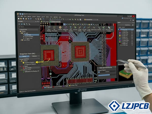
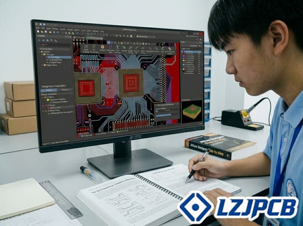
Can ChatGPT Assist With PCB Design?
While ChatGPT can’t directly create PCB designs, it offers valuable support throughout the design process. As someone who manages PCB design16 projects daily, I’ve explored how AI assistants17 like ChatGPT can complement traditional design workflows. Let me outline the specific ways ChatGPT can help PCB designers, along with important limitations to keep in mind.
ChatGPT’s PCB Design Capabilities and Limitations
ChatGPT offers several valuable capabilities for PCB designers while having clear limitations that require human expertise to overcome. Understanding these boundaries helps set appropriate expectations for AI assistance in your design workflow.
| Aspect | ChatGPT Can | ChatGPT Cannot | Human Input Required |
|---|---|---|---|
| Design Files | Explain file formats, discuss structure | Generate actual Gerber, ODB++, or native CAD files | Using PCB CAD software to create physical designs |
| Component Selection | Suggest components based on specs, compare options | Check real time availability, pricing | Verifying recommendations against current market conditions |
| Layout Guidelines | Provide design rules, calculate trace width requirements | Create actual layouts, perform DRC checks | Implementing guidelines in CAD software |
| Signal Integrity | Explain concepts, provide formulas, suggest best practices | Perform actual simulations | Running simulation software, interpreting complex results |
| Thermal Analysis | Discuss thermal considerations, calculate basic parameters | Perform detailed thermal simulation | Using specialized thermal analysis18 tools |
| Design Reviews | Suggest checklist items, explain common issues | Visually inspect designs, identify specific layout issues | Performing actual design reviews19 with CAD tools |
| Documentation | Generate descriptions, explain design decisions | Create formal documentation20 with drawings | Preparing complete documentation20 packages |
| Manufacturing Support | Explain processes, suggest DFM improvements | Generate manufacturing files | Preparing files for fabrication and assembly |
Component Selection and Research
ChatGPT excels at helping designers research and compare components based on specifications. For example, if you need to select a voltage regulator with specific input range, output current, and package requirements, ChatGPT can suggest appropriate component families and explain tradeoffs between options.
I recently used ChatGPT to compile a list of potential alternatives when a client’s design used components affected by supply chain shortages21. It quickly provided several options with similar specifications that I could then verify for availability and pricing. This significantly accelerated the component research process.
However, ChatGPT cannot access real time inventory information or current pricing, so all component suggestions require verification. Its component knowledge also has a cutoff date, meaning it may not be aware of the newest components on the market.
Design Rule Calculations
ChatGPT performs well when calculating design parameters like trace width requirements, impedance values, or power dissipation. For example, it can calculate the appropriate trace width for a given current based on IPC standards or determine microstrip impedance values for controlled impedance routing.
When designing a power distribution network, I asked ChatGPT to calculate minimum trace widths for various current requirements across different copper weights. It quickly provided a comprehensive table based on IPC-2152 standards that I could reference during layout.
These calculations save time but should always be verified against industry standards or simulation tools for critical applications. ChatGPT may occasionally make mathematical errors or apply formulas incorrectly, especially for complex scenarios.
Layout Strategy and Component Placement
ChatGPT can provide strategic guidance on component placement and routing approaches. For example, it can suggest optimal arrangements for sensitive analog circuits, recommend grounding strategies for mixed signal designs, or provide guidelines for high speed differential pair routing.
For a recent IoT device design, I asked ChatGPT for recommendations on partitioning the board for RF isolation. It provided a logical approach for separating digital, power, and RF sections with appropriate grounding strategies that informed my initial placement decisions.
However, ChatGPT cannot see your actual design or make specific recommendations based on your particular layout challenges. Its advice remains general rather than tailored to specific design files.
Technical Documentation Support
ChatGPT excels at generating documentation20 content such as design rationales, assembly notes, or test procedures. It can help articulate design decisions and create clear explanations for manufacturing partners or team members.
When preparing documentation20 for a complex industrial controller board, I used ChatGPT to help draft sections explaining the power sequencing requirements and test procedures. This accelerated the documentation20 process while ensuring comprehensive coverage of technical details.
While helpful for content generation, ChatGPT cannot create complete documentation20 packages that include actual design files, drawings, or test reports. Human review is essential to ensure accuracy.
Troubleshooting and Problem Solving
ChatGPT can assist with troubleshooting22 design issues by suggesting potential causes and solutions based on described symptoms. It can help brainstorm approaches to design challenges like noise reduction, EMI mitigation, or thermal management.
During design review for a motor controller, we encountered unexpected noise issues in sensor readings. I described the symptoms to ChatGPT, which suggested several potential causes including ground loops, inadequate decoupling, and inductive coupling from nearby power traces. This helped guide our investigation to identify and resolve the issue.
However, ChatGPT cannot diagnose specific issues in your actual design without seeing it, and its suggestions require validation through testing or simulation.
Learning and Skill Development
ChatGPT serves as an excellent learning resource for PCB designers looking to expand their knowledge. It can explain complex concepts, suggest learning resources23, and provide step-by-step explanations of design techniques.
When mentoring a junior designer on high speed design principles, I used ChatGPT to generate clear explanations of concepts like impedance control, return path analysis, and signal reflections. These explanations complemented formal training materials and helped build understanding of the underlying principles.
While valuable for explanations, ChatGPT sometimes oversimplifies complex topics and may occasionally provide outdated information, requiring verification against current industry practices.
Project Planning and Management
ChatGPT can assist with planning PCB design16 projects by helping create timelines, identify dependencies, and develop checklists for design reviews19 or manufacturing preparation.
For a complex multi board system design, I used ChatGPT to help develop a comprehensive design review checklist specific to the project requirements. This ensured we covered all critical aspects during review and reduced the risk of overlooking important design considerations.
However, ChatGPT lacks knowledge of your specific team capabilities, vendor relationships, or organizational processes that would affect realistic planning.
Manufacturing and Assembly Considerations
ChatGPT can provide guidance on design for manufacturing24 (DFM) and design for assembly (DFA) principles to improve producibility. It can explain manufacturing processes and suggest design approaches to reduce costs or improve yield.
When preparing a design for offshore manufacturing, I consulted ChatGPT about specific DFM considerations for the vendor’s process capabilities. It provided a comprehensive list of design guidelines addressing minimum feature sizes, preferred pad geometries, and testability considerations that improved our manufacturing preparation.
However, ChatGPT cannot generate actual manufacturing files like Gerbers, drill files, or pick and place data, nor can it perform DFM checks on your specific design files.
Conclusion
While ChatGPT cannot create actual PCB designs or generate manufacturing files, it provides valuable support for component selection, design calculations, layout strategy, and documentation. Learning PCB design requires 2-3 months for basics and 1-3 years for mastery, with salaries ranging from $45,000 for beginners to $120,000+ for experts depending on location, specialization, and industry.
-
Explore comprehensive resources to kickstart your PCB design journey and gain essential skills. ↩ ↩ ↩ ↩ ↩ ↩
-
Understanding schematic capture is crucial for PCB design; find detailed guides to master this skill. ↩ ↩ ↩
-
DFM considerations can save time and costs; learn how to implement them effectively in your designs. ↩
-
Thermal management is crucial for reliability; explore resources that provide insights into effective strategies. ↩ ↩
-
High speed design techniques are complex; find expert resources to navigate this challenging area. ↩
-
Signal integrity is vital for performance; explore resources that explain its significance in PCB design. ↩ ↩ ↩
-
KiCad is a popular tool; explore its features to see how it can aid your PCB design process. ↩
-
Altium Designer offers advanced capabilities; discover why it’s favored by professionals in the industry. ↩
-
Learn effective component selection strategies to enhance your PCB designs and ensure reliability. ↩
-
Developing a PCB mindset is key to success; find resources that help cultivate this multidisciplinary approach. ↩
-
Understanding salary benchmarks can help you negotiate better compensation or set competitive offers. ↩ ↩ ↩
-
Learn how location impacts compensation and job opportunities in PCB design. ↩
-
Identifying high paying industries can guide your career choices and specialization. ↩
-
Find out how certifications can enhance your qualifications and salary prospects. ↩
-
Learn how this integration is becoming essential for modern PCB design roles. ↩
-
Explore comprehensive guides and tutorials to enhance your PCB design skills. ↩ ↩
-
Discover innovative ways AI can streamline your PCB design process. ↩
-
Explore tools that can help you perform detailed thermal analysis for your PCBs. ↩
-
Get insights on creating a thorough design review checklist for your projects. ↩ ↩
-
Learn how to create effective documentation for your PCB designs. ↩ ↩ ↩ ↩ ↩ ↩
-
Find strategies to effectively navigate component shortages in PCB design. ↩
-
Find effective troubleshooting techniques to resolve common PCB design problems. ↩
-
Explore valuable resources to expand your knowledge in PCB design. ↩
-
Understand the principles of DFM to improve your PCB designs. ↩