Skip to content
 Staring at a bare PCB and a pile of tiny components can feel overwhelming. With dozens or hundreds of parts that must be placed precisely, and the risk of irreversible damage if mistakes are made, many engineers and hobbyists feel paralyzed before they begin.
PCB assembly involves preparing the bare board, applying solder paste to connection pads, precisely placing components using manual or automated equipment, soldering components through reflow or wave soldering, inspecting for defects, testing functionality, and cleaning the finished assembly.
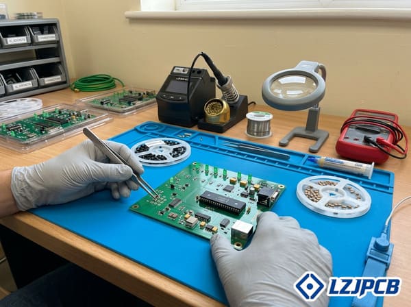
The process of bringing a PCB to life through assembly transforms a simple fiberglass board with copper traces into a functioning electronic system. I’ve overseen thousands of PCB assemblies during my career, from simple one layer designs to complex multilayer boards with thousands of components. Whether you’re planning to assemble boards yourself or work with a manufacturing partner like us at LZJPCB, understanding the assembly process is crucial for successful electronic product development.
What Are the Essential Steps in Surface Mount PCB Assembly?
Surface mount technology has revolutionized electronics manufacturing, but the precision required can be intimidating. One misaligned component or improper temperature profile can render an entire board useless.
The essential steps in surface mount PCB assembly are: stencil printing solder paste onto PCB pads, component placement using pick and place equipment, reflow soldering in a controlled temperature oven, inspection for defects using AOI or X ray systems, and functional testing to verify performance.
Surface Mount Technology (SMT) has become the dominant assembly method for modern electronics due to its efficiency and ability to create compact, high performance devices. The process is highly optimized but requires precision at every stage. I remember when our facility first transitioned from primarily through hole to SMT assembly, the learning curve was steep, but the benefits were immediately apparent.
The SMT Assembly Process in Detail
Each step in the SMT assembly process requires careful control and monitoring to ensure quality results. Even small deviations in process parameters can lead to defects that may not be immediately obvious but could cause device failure later.
| Process Step | Equipment Used | Critical Parameters | Common Challenges |
|---|---|---|---|
| Solder Paste Application | Stencil printer | Stencil thickness, print pressure, print speed | Insufficient paste, smearing, misalignment |
| Component Placement | Pick and place machine | Component orientation, placement accuracy, placement force | Missing components, misalignment, polarity errors |
| Reflow Soldering | Reflow oven | Temperature profile, conveyor speed, atmosphere control | Cold solder joints, tombstoning, bridging |
| Inspection | AOI system, X ray inspection | Detection thresholds, camera resolution | False positives, hidden defects, solder voids1 |
| Functional Testing | Custom test fixtures, ICT, flying probe | Test coverage, contact reliability | Test accessibility, intermittent faults |
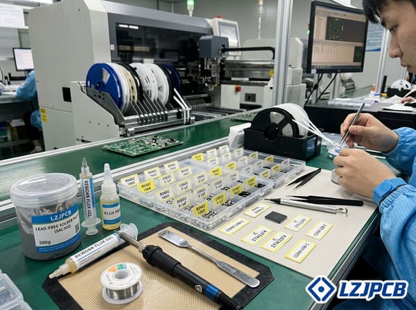
The solder paste application2 is particularly critical, I often tell our new technicians that this step determines 70% of assembly quality. The paste must be applied in precisely the right amount, too little causes weak connections, while too much can create bridges between adjacent pads. The viscosity of the paste must be carefully controlled, which means monitoring temperature and humidity in the production environment.
Component placement accuracy has become increasingly demanding as electronics have miniaturized. Modern smartphones contain components as small as 01005 (0.4mm × 0.2mm), which are barely visible to the naked eye. Our pick and place machines must position these tiny parts with accuracy measured in microns, all while operating at speeds of up to 60,000 components per hour.
The reflow soldering3 process requires precise thermal management. The board passes through multiple heating zones in the reflow oven, following a specific temperature profile with several stages: preheat, thermal soak, reflow, and cooling. Each stage serves a specific purpose, from activating the flux to forming proper intermetallic bonds between component leads and PCB pads. We regularly perform thermal profiling4 to ensure our reflow ovens maintain the correct temperatures throughout the process.
Post assembly inspection is critical for quality assurance. Our Automated Optical Inspection (AOI)5 systems use high resolution cameras and sophisticated algorithms to detect defects like misaligned components, insufficient solder, or solder bridges. For components with hidden connections like BGAs (Ball Grid Arrays), we use X ray inspection to see through the package and verify the integrity of solder joints underneath.
What is PCB Assembly Equipment?
Starting a PCB assembly operation requires significant investment in specialized equipment. Without understanding what’s needed and how each machine functions, companies risk purchasing inadequate tools or overspending on unnecessary capabilities.
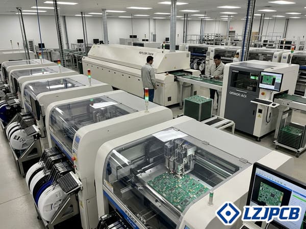
PCB assembly equipment includes solder paste printers, pick and place machines, reflow ovens, wave soldering systems, selective soldering equipment, AOI and X ray inspection systems, and various testing devices. For high volume production, these machines are typically connected in automated assembly lines.
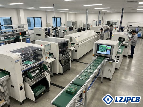
The evolution of PCB assembly equipment6 has been remarkable over my career. When I started in this industry, much of the assembly process was still manual or semi automated. Today, our production lines at LZJPCB feature highly automated equipment that can place tiny components with incredible speed and accuracy while maintaining consistent quality.
Key Equipment in PCB Assembly Operations
The right equipment selection depends on production volume, component types, board complexity, and quality requirements. I’ve helped multiple clients determine their equipment needs based on these factors, and the decision significantly impacts production capability and cost structure.
| Equipment Type | Function | Selection Considerations | Approximate Cost Range |
|---|---|---|---|
| Solder Paste Printer | Applies solder paste to PCB | Printing area, alignment accuracy, cycle time | $15,000 – $150,000 |
| Pick and Place Machine | Places components on the PCB | Placement speed, component range, accuracy | $30,000 – $500,000+ |
| Reflow Oven | Melts solder paste to form connections | Number of heating zones, temperature control, conveyor width | $10,000 – $100,000 |
| Wave Soldering Machine | Solders through hole components | Wave width, temperature control, flux application | $20,000 – $150,000 |
| Selective Soldering System | Precisely solders specific areas | Number of solder pots, positioning accuracy | $50,000 – $250,000 |
| AOI System | Inspects boards for visual defects | Camera resolution, inspection area, defect detection capabilities | $30,000 – $200,000 |
| X-ray Inspection System | Inspects hidden solder joints | Magnification range, detection capabilities | $80,000 – $500,000 |
| In Circuit Tester7 | Tests electrical functionality | Test point density, fixture cost, test coverage | $50,000 – $300,000+ |
Modern solder paste printers8 have evolved significantly from their early counterparts. Our latest models include automatic stencil cleaning, vision alignment systems, and solder paste height measurement capabilities. These features help maintain consistent paste deposition, which is crucial for reliable solder joints, especially with fine pitch components.
Pick and place machines are at the heart of SMT assembly. Entry level machines might place 5,000 components per hour, while high end models can exceed 100,000 components per hour with multiple placement heads working simultaneously. The machines use vision systems to accurately align components, correct for placement offsets, and verify part orientation before placement.
Reflow ovens have also become more sophisticated, with more heating zones for better profile control and features like nitrogen atmosphere capability for higher quality soldering. Our newest reflow systems include real time process monitoring that can detect and correct profile deviations during production.
For through hole components, wave soldering remains an efficient solution. Modern wave soldering machines feature programmable wave heights, dual wave systems (for better penetration of plated through holes), and sophisticated flux application systems that minimize waste and environmental impact.
Inspection equipment has seen some of the most dramatic improvements. Today’s AOI systems can detect defects that would be invisible to human inspectors, while advanced algorithms reduce false positives that plagued earlier generations of equipment. X-ray inspection systems now provide 3D imaging capabilities that allow us to examine solder joints layer by layer in complex assemblies.
What Are the Materials Used in PCB Assembly?
Selecting the wrong materials for PCB assembly can lead to manufacturing defects, premature product failure, or non compliance with environmental regulations9, costly mistakes that can delay product launches and damage company reputations.
PCB assembly materials include solder paste (typically tin silver copper alloy), flux (to clean and prepare surfaces), various component types (ICs, resistors, capacitors, etc.), cleaning agents, conformal coatings, underfill materials for structural support, and thermal interface materials for heat management.
The transition to lead free soldering10 was one of the most significant material changes I’ve experienced in this industry. When RoHS regulations were implemented, we had to completely rethink our material selections and process parameters. The higher melting point of lead free solders required changes to everything from the reflow profile to the thermal ratings of components.
Critical Materials in the PCB Assembly Process
Material selection impacts not just the assembly process but also the long term reliability of the finished product. I’ve seen cases where an apparently minor change in material specification led to significant field failures months or years later.
| Material Category | Common Types | Key Properties | Application Considerations |
|---|---|---|---|
| Solder Paste | SAC305, SAC387, SN100C | Melting temperature, wetting characteristics, mechanical strength | Component temperature ratings, operating environment, reliability requirements |
| Flux | No clean, water soluble, rosin | Activation level, cleaning requirements, residue characteristics | Cleanliness requirements, potential for corrosion, test point access |
| Components | Active (ICs, transistors), Passive (resistors, capacitors) | Package type, temperature rating, moisture sensitivity | Storage conditions, handling requirements, thermal considerations |
| Cleaning Agents | Aqueous, semi aqueous, solvent based | Cleaning effectiveness, environmental impact, material compatibility | Residue types, regulatory compliance, equipment compatibility |
| Conformal Coating | Acrylic, silicone, polyurethane, parylene | Protection level, application method, rework difficulty | Operating environment, moisture exposure, temperature range |
| Underfill | Epoxy based, reworkable, no flow | Flow characteristics, curing requirements, adhesion strength | Component type, reliability requirements, rework needs |
| Thermal Interface Materials | Thermal paste, gap fillers, phase change materials | Thermal conductivity, compression properties, long term stability | Heat dissipation requirements, assembly process, maintenance needs |
Solder paste composition dramatically affects assembly quality. The industry standard for lead free assembly is SAC305 (96.5% tin, 3% silver, 0.5% copper), but we sometimes use specialized alloys for specific applications. For high temperature environments, higher melting point alloys might be required, while cost sensitive products might use alloys with lower silver content to reduce material costs.
Flux selection depends on both process requirements and the final operating environment of the product. No clean fluxes are popular because they eliminate the cleaning step, but their residues can interfere with electrical testing and may not be acceptable for all applications. Water soluble fluxes provide excellent cleaning capability but require thorough washing after soldering to prevent corrosion.
Component selection involves not just electrical specifications but also packaging considerations. Modern components come in a vast array of package types, each with specific handling and assembly requirements. For example, moisture sensitive devices must be carefully managed to prevent damage during reflow, while fine pitch components require precise paste printing and placement.
Cleaning materials have evolved significantly due to environmental regulations9. The chlorofluorocarbon (CFC) cleaners once common in electronics manufacturing have been replaced by more environmentally friendly alternatives. However, these newer cleaning agents11 often require different equipment and process parameters to achieve the same level of cleanliness.
Protective materials like conformal coatings12 are increasingly important as electronics are deployed in harsh environments. At LZJPCB, we apply various coating types depending on the expected operating conditions, silicone coatings for high temperature applications, acrylic for general protection, and parylene for the most demanding environments requiring thin, pinhole free coverage.
For high reliability applications, underfill materials13 provide mechanical support to delicate components like BGAs and chip scale packages. These epoxy based materials flow under the component after soldering and cure to form a solid support that protects solder joints from mechanical stress and thermal cycling.
Conclusion
PCB assembly transforms a bare circuit board into a functional electronic system through precise component placement and soldering. Whether using automated equipment or hand assembly, success requires careful preparation, proper materials, and attention to detail throughout the process of creating reliable electronic devices.
-
Solder voids can lead to device failure; learning about them helps in implementing better inspection and quality control measures. ↩
-
Understanding solder paste application is crucial as it significantly impacts assembly quality, affecting the entire manufacturing process. ↩
-
Reflow soldering is a critical step in PCB assembly; mastering it ensures strong solder joints and reliable electronic devices. ↩
-
Thermal profiling ensures optimal temperature management during reflow soldering, crucial for achieving high-quality solder joints. ↩
-
AOI is essential for quality assurance in PCB manufacturing, helping to detect defects early and improve overall product reliability. ↩
-
Understanding PCB assembly equipment is crucial for optimizing production efficiency and ensuring quality in electronic manufacturing. ↩
-
Learn about In Circuit Testers and their importance in verifying electrical functionality in PCBs. ↩
-
Explore how solder paste printers enhance the quality of solder joints and improve assembly accuracy. ↩
-
Stay informed about environmental regulations to ensure compliance and sustainability in manufacturing. ↩ ↩
-
Explore the advantages of lead free soldering, especially in compliance with environmental regulations. ↩
-
Learn about cleaning agents to ensure compliance and effectiveness in the PCB assembly process. ↩
-
Discover how conformal coatings protect electronics in harsh environments, enhancing reliability. ↩
-
Explore how underfill materials provide mechanical support and enhance reliability in PCBs. ↩