Skip to content
 LZJPCB China Manufacturing Factory
LZJPCB operates three manufacturing factory in China, forming a vertically integrated PCB Manufacturing and PCB Assembly supply chain. Our Shenzhen headquarters (established 2006, 6,000 m²) handles PCBA production and global sales; our Jiangxi factory (established 2010, 15,000 m²) specializes in 1–40 layer rigid PCBs with a monthly capacity exceeding 50,000 m²; and our Changsha factory (established 2024, 3,000 m²) provides precision PCBA assembly. All three sites are certified to ISO 9001:2015, ISO 14001:2015, and IATF 16949:2016, with UL recognition for finished boards.

Senior Electronics Engineer
| Facility | Location | Established | Area | Core Function | Monthly Capacity |
|---|---|---|---|---|---|
| Shenzhen HQ | Bao'an District, Shenzhen, Guangdong | 2006 | 6,000 m² | PCBA Manufacturing, FPC Production, Global Sales HQ | 200M+ component placements |
| Jiangxi PCB Factory | Ji'an, Jiangxi Province | 2010 | 15,000 m² | Rigid PCB Manufacturing (1–40 layers) | 50,000+ m² and 2,500+ models |
| Changsha PCBA Center | Changsha, Hunan Province | 2024 | 3,000 m² | Precision PCBA Assembly | (disclosed on inquiry) |
Shenzhen Headquarters: PCBA & FPC Manufacturing Hub
LZJPCB Shenzhen headquarters, in Tantou Third Industrial Zone, Songgang Street, Bao’an District, Shenzhen has been the company’s main hub since 2006. This 6,000 m² facility is home to three key units: a PCB assembly factory, set up in 2014, a flexible circuit factory for FPC, which opened in 2022, and the teams handling global sales and engineering. So, Shenzhen is where LZJPCB mainly ships its exports, to over 50 countries.

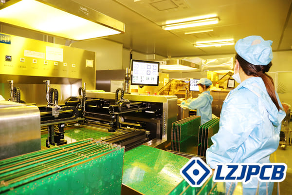
Shenzhen PCBA Factory — Equipment & Capability
The Shenzhen PCBA factory operates fully automated SMT lines equipped with YAMAHA high-speed and multi-functional pick-and-place machines, GKG automatic solder paste printers, 10–12 zone reflow ovens (Jingtuo), wave soldering machines, and CNC depaneling routers. Quality control is enforced through 3D SPI, online AOI, X-Ray inspection, intelligent first-article inspection systems, and BGA rework stations. Daily soldering capacity reaches 8 million solder joints.
Shenzhen SMT Process Capability
- smallest component we can package is the 01005 chip
- Our smallest BGA pitch is 0.35 mm
- When it comes to IC placement, we achieve an accuracy of ±0.03 mm
- For general components accuracy is ±0.04 mm
- We can work with PCB size ranging from 50×50 mm to 774×710 mm
- PCB thickness range is between 0.3 mm and 6.5 mm
- The types of boards we support include POP, standard rigid, FPC, rigid-flex, and metal-core
- Prototype lead time is quick turn 24 hours for single or double-sided, and 48 hours for small batches
Shenzhen FPC Factory — Flexible Circuit Production
The LZJPCB Flex PCB factory in Shenzhen occupies 2,500 m² of Class-100,000 cleanroom space and produces 8,000 m² of flexible circuits per month. The factory manufactures 1–8 layer FPCs and rigid-flex boards with a minimum trace width of 2 mil (0.05 mm), minimum mechanical hole diameter of 0.1 mm, and laser hole diameter of 0.05 mm. First-pass yield consistently exceeds 98%. Typical applications include medical devices, automotive electronics, telecommunications equipment, instrumentation, and smart wearables.
FPC Process Capability
- Layer count: 1 to 8 layers, both FPC and rigid-flex.
- Maximum finished board size is 250 × 1000 mm.
- Board thickness varies – for FPC, it’s between 0.06-0.4 mm, and for rigid-flex, it’s 0.25-6.0 mm.
- Copper thickness options are 12, 18, 35, 70, and 105 µm.
- Minimum trace/spacing is 0.03 / 0.03 mm for FPC, and 0.1 / 0.1 mm for rigid-flex.
- Surface finish options include ENIG, immersion silver, immersion tin, gold plating, OSP, and ENEPIG.
- Impedance control range is 50 Ω – 120 Ω.
Jiangxi PCB Factory: Rigid PCB Manufacturing Specialist
The LZJPCB Jiangxi PCB factory, located in Ji’an City, Jiangxi Province, was established in 2010 and relocated to its current 15,000 m² site in 2018. The factory employs over 200 workers and engineers and serves as the source manufacturing node of LZJPCB’s vertically integrated supply chain. Jiangxi specializes in high-multilayer, high-frequency, metal-core, rigid-flex, and HDI printed circuit boards, supporting layer counts from 1 to 40.
Jiangxi Production Lines & Equipment
The Jiangxi facility has production lines dedicated to drilling, LDI, or Laser Direct Imaging, and other processes like CCD exposure, etching, electroplating, solder mask application, surface finish processing, AOI inspection, electrical testing, and CNC routing. They get their raw laminate materials from top suppliers, including Kingboard, Shengyi, and ITEQ, which meet UL and RoHS standards. And every PCB goes through 100% electrical testing and AOI verification before it ships.
Jiangxi PCB Process Capability
| Parameter | Prototype | Mass Production |
|---|---|---|
| Layer count | 1–40 layers | 1–32 layers |
| Board thickness | 0.2–17.5 mm | 0.2–17.5 mm |
| Minimum mechanical hole | 0.1 mm | 0.1 mm |
| Minimum laser hole | 0.075 mm (3 mil) | 0.075 mm (3 mil) |
| HDI structures | 1+N+1, 2+N+2, 3+N+3 | 1+N+1, 2+N+2, 3+N+3 |
| Minimum trace/spacing | 3 / 3 mil | 3 / 3 mil |
| Impedance tolerance | ±5% | ±5% |
| Maximum copper thickness | 12 oz | 12 oz |
| Maximum aspect ratio | 16:1 | 16:1 |
| Maximum panel size | 650 × 2000 mm | 650 × 2000 mm |
Jiangxi PCB Material and Surface Finish Options
- Substrate materials include FR-4, high-temperature FR-4, Rogers materials like RO4350B and RO4003C, halogen-free options, metal-core materials with aluminum or copper, and other types such as RCC, PTFE, Nelco, and hybrid stack-ups.
- Surface finishes are available in several forms: HASL, lead-free HASL, ENIG, immersion silver, electrolytic gold, immersion tin, gold fingers, and combinations like ENIG with OSP.
- Special processes that can be applied include blind or buried vias, back-drilling, countersink holes, heavy copper plating, bare copper, the production of ultra-long or ultra-thin boards, embedded resistors, embedded capacitors, and stepped gold fingers.
Jiangxi Lead Time Commitments
- Single or double-sided PCBs can be delivered in 12 hours with expedited service
- For 4-layer PCBs, we offer 24-hour expedited delivery
- And 6-layer PCBs take a bit longer, with delivery in 48 hours
- Our on-time delivery rate is at least 99 percent
Changsha PCBA Precision Assembly Center
The LZJPCB Changsha facility, set up in October 2024, covers 3,000 m² and is used for PCBA precision assembly. It’s in Changsha, Hunan Province. By having this center, LZJPCB can now serve customers who need more than one supply chain option in China. The facility makes electronics for cars, medical devices, and industrial controls. It follows the same quality systems as the Shenzhen headquarters, like IATF 16949 and ISO 13485.
LZJPCB first opened a sales office in Changsha back in 2015. So, the company has been working in the area for about a decade, which helps with finding workers and suppliers.
Why LZJPCB’s Three Factories China Matters to OEM Buyers
LZJPCB operates 5 assembly technologies in parallel, chosen based on your board’s components, volume, and environmental requirements:
1. Vertical Integration: PCB to FPC to PCBA Under One Group
LZJPCB controls the full electronics manufacturing chain in-house: rigid PCBs are fabricated in Jiangxi, flexible circuits in Shenzhen, and final PCBA assembly in either Shenzhen or Changsha. This eliminates the typical inter-vendor handoffs that cause delays and quality discrepancies in multi-supplier PCBA projects.
2. Multi-Site Redundancy Within China
Operating two PCBA sites (Shenzhen and Changsha) provides domestic redundancy. If a customer’s program requires capacity reallocation due to demand spikes, regional logistics preferences, or business continuity planning, LZJPCB can shift production between sites without changing suppliers.
3. Certifications Applied Consistently Across All Sites
- ISO 9001:2015 — Quality Management System
- ISO 14001:2015 — Environmental Management System
- ISO 13485:2016 — Medical Device Quality System
- IATF 16949:2016 — Automotive Electronics Quality Management
- UL Recognition — Finished PCB safety certification (US)
- RoHS / REACH Compliance — EU environmental standards
4. Patent Portfolio
LZJPCB holds over 20 granted patents covering invention, utility, and design categories, primarily in PCB manufacturing process improvements and PCBA assembly tooling.
Frequently Asked Questions About LZJPCB's China Factories
How many PCB and PCBA factories does LZJPCB operate in China?
LZJPCB operates three manufacturing facilities in China: the Shenzhen headquarters (PCBA and FPC, 6,000 m², established 2006), the Jiangxi PCB factory in Ji’an (rigid PCB, 15,000 m², established 2010), and the Changsha PCBA precision assembly center (3,000 m², established 2024). A fourth facility in Jakarta Indonesia (4,000 m², established 2025) extends the network internationally.
Where is LZJPCB's main PCB factory located?
LZJPCB’s main rigid PCB manufacturing factory is located in Ji’an, Jiangxi Province, China. The 15,000 m² facility has been in operation since 2010 and produces 1–40 layer PCBs with a monthly capacity exceeding 50,000 m² across more than 2,500 unique part numbers.
What is the maximum layer count LZJPCB can manufacture?
LZJPCB’s Jiangxi factory manufactures rigid PCBs from 1 to 40 layers for prototype orders and up to 32 layers for mass production. The factory supports HDI structures including 1+N+1, 2+N+2, and 3+N+3 stack-ups, with minimum laser via diameter of 0.075 mm and minimum trace/spacing of 3/3 mil.
How fast can LZJPCB deliver PCB prototypes from China?
LZJPCB offers expedited prototype delivery from its Jiangxi PCB factory, with turnaround times as short as 12 hours for single or double-sided boards, 24 hours for 4-layer boards, and 48 hours for 6-layer boards. And for PCBA prototypes from the Shenzhen factory, you’re looking at 24 hours for single or double-sided assemblies, and 48 hours for small-batch orders, which is pretty standard. The on-time delivery rate across all China sites is over 99%, so you can count on getting your prototypes on time.
Are LZJPCB's China factories certified for automotive and medical applications?
Yes. All LZJPCB China facilities operate under IATF 16949:2016 (automotive electronics) and ISO 13485:2016 (medical devices) quality management systems. Finished PCBs carry UL recognition, and all materials comply with RoHS and REACH environmental regulations.
What industries does LZJPCB serve from its China factories?
LZJPCB’s China factories supply PCB and PCBA products to nine primary industries: automotive electronics, medical devices, renewable energy, industrial control, power electronics, instrumentation, artificial intelligence hardware, telecommunications, and smart wearables. Products ship to over 50 countries.
Can LZJPCB handle the full PCBA process including component sourcing?
Yes. LZJPCB provides one-stop PCBA service from its China factories, covering PCB fabrication, BOM analysis and component sourcing, SMT and DIP assembly, functional testing, and final packaging. Components are sourced exclusively from original manufacturers and authorized distributors with full traceability, and all incoming materials pass IQC inspection before entering production.