Skip to content
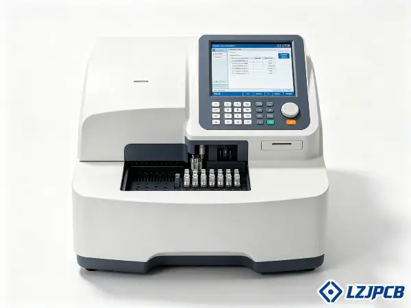
 Medical PCB Assembly and Manufacturing
LZJPCB is ISO 13485:2016 certified for medical PCB assembly. Advanced PCBs for medical devices meeting strict FDA compliant and medical grade standards.
TL;DR
Medical PCBs are a matter of patient safety. They have to follow IPC Class 3 manufacturing standards and ISO 13485 quality systems. When you pick a supplier, check their certifications and supply chain.
Our Medical Device PCB Case Studies
The engineering value of medical PCBs is demonstrated through real-world application validation, not just a list of specifications. The following cases cover all typical medical application scenarios.


Why Medical PCB Have Stricter Standards
The strict standards for medical-grade PCBs stem from one core premise: PCB failure can directly cause patient injury or death.

- IPC-6012EM sets the rules for the thickness of holes in copper on medical-grade PCBs. For medical Class 3, the minimum is 20 µm. But industrial Class 2 is thinner at just 15 µm. This is based on IPC-6012EM, “Medical and Rigid Board Performance Sub-specification,” §3.3.2, a standard that covers both medical and military uses.
- IEC 60601-1 lists the limits for patient leakage current. Type B parts must remain at or below 100 µA (both AC and DC) during normal use. If there is a single fault, that limit goes up to 500 µA for AC and DC.
- Under FDA 21 CFR Part 820, medical device makers have to set up a full quality management system. It has to handle design control and production processes. Change control is part of the deal too. According to the QMSR update from February 2024, these rules will become fully effective on February 2, 2026.
- ISO 13485:2016 §7.5.9 says you have to track a product through its whole life cycle. This means every batch needs material and process records that lead back to the original raw material certificates.
PCB Functions in Medical Devices
In medical devices, PCBs handle four main functions: signal acquisition, processing, transmission, and executive control.
- An electrocardiogram device’s PCB captures bioelectrical signals, which are tiny, in the range of 0.1-5 mV. The signal integrity requirements here are much stricter than those for industrial electronics. And that’s a challenge, because these signals are easily disrupted.
- A pacemaker’s PCB works continuously at 37°C, inside the body, surrounded by fluids. It needs to last a long time – the design target is at least 100,000 hours of operation without failing.
- MRI signal processing boards have to keep signals stable at high frequencies, 64 MHz to 300 MHz, and resist interference from magnetic fields. This is important for getting accurate images.
- A surgical robot’s control board has to respond in real time, with delays of just a few milliseconds. Any delay in PCB transmission can affect how accurately the robot moves.
There are significant differences in the application tier of medical device PCBs, with different tiers corresponding to different reliability requirements:
| Equipment category | representative device | IPC class reference | key PCB requirements |
|---|---|---|---|
| Implantable or life support | pacemakers, defibrillators, neurostimulators | IPC Class 3 (IPC-6012EM) | full traceability, ISO 10993 biocompatibility, Parylene coating |
| High-risk diagnostic | MRI signal boards, CT image acquisition cards | IPC Class 3 | high layer counts (up to 20–30 layers), low-loss base materials, EMI shielding |
| Medium-risk diagnostic | ultrasound probe drivers, X-ray control boards | IPC Class 2–3 | controlled impedance, thermal management |
| Monitoring | ECG monitors, pulse oximeters, blood pressure monitors | IPC Class 2–3 | leakage current control, waterproof coating |
| Consumer-grade health tracking | sports wristbands (non-regulated medical devices) | IPC Class 2 | RoHS 2 (2011/65/EU) compliant |
Note: Consumer-grade health tracking devices are not classified as medical devices regulated by the FDA or EU MDR and should not be analyzed together with the above-regulated devices.
Why IPC Class 3 Is the Medical Standard
IPC Class 3 represents the highest level of workmanship quality, applicable to devices where failure could put lives at risk. This requires rigorous inspection and adherence to the strict process requirements outlined in IPC-6012EM. According to IPC-A-610H §1.3, Class 3 is suited for devices that demand continuous performance or performance on demand, such as life support systems, implantable devices, and high-risk surgical equipment.
The following comparison highlights the core differences between IPC Class 2 and Class 3:
| Indicator | IPC Class 2 | IPC Class 3 (including IPC-6012EM) |
|---|---|---|
| Minimum hole copper thickness | 15 µm | average 20 µm with local minimum ≥ 18 µm |
| Solder joint acceptance criteria | IPC-A-610H §8 Class 2 | IPC-A-610H §8 Class 3 (more stringent coverage requirements) |
| Visual acceptance | IPC-A-600K Class 2 | IPC-A-600K Class 3 |
| Traceability | recommended | mandatory per ISO 13485:2016 §7.5.9 |
| Typical applicable devices | diagnostic instruments, laboratory equipment | implantable devices, life support equipment, high-risk surgical equipment |
It’s worth noting that both IPC Class 2 and Class 3 are voluntary industry standards, the FDA doesn’t mandate IPC Class 3 certification, as outlined in FDA Voluntary Consensus Standards, FDASIA §587.
The specific applicable class is determined through risk assessment and should be confirmed in writing in contract documents, which is a more reliable approach than simply going by device type intuition.
Diagnostic equipment, like ultrasound or imaging workstations, usually falls under Class 2, and life-support equipment typically requires Class 3.
Medical vs Industrial PCB Differences
Medical PCBs are completely different from industrial PCBs. They vary in terms of standards systems, traceability requirements, and material specifications. Industrial specs just can’t replace medical specs.
The following table shows the differences between medical PCBs and industrial PCBs:
| Dimension | Industrial PCB | Medical PCB |
|---|---|---|
| Quality management system | ISO 9001:2015 (generic QMS requirements) | ISO 13485:2016 (medical device dedicated QMS, an independent and complete standard; ISO 9001 is not required simultaneously) |
| Manufacturing specification | IPC Class 1–2 | IPC Class 2–3; high-risk devices must comply with IPC-6012EM |
| Safety standard | IEC 62368-1 | IEC 60601-1:2005+AMD2:2020 plus family of collateral standards |
| Traceability | per project requirements | full batch-level traceability |
| Regulatory compliance | RoHS, CE | FDA 21 CFR Part 820 / EU MDR 2017/745 |
| Change control | internal ECO process | formal design change control (DCN/ECO); material substitution requires approval |
| Layer count range | typically 2–12 layers, typically 4–20 layers | high-end imaging equipment may use higher layer counts (refer to IPC-2221B Annex A) |
| Trace width tolerance | approximately ±15–20% (industry practice) | approximately ±10% (industry practice; specific values should be based on IPC-6012E Class 3 fabrication precision grade and confirmed in writing in the contract) |
Supplementary note: Consumer electronic PCBs have to meet some mandatory standards, like RoHS 2, REACH, and UL 94 flammability ratings. But for medical PCBs, it’s different. They need to meet not just these standards, but also medical-grade reliability standards, biocompatibility requirements, and regulatory documentation obligations. And that’s a significant added layer of complexity.
Medical Grade Material Selection
Substrate selection for medical PCBs directly determines the device’s electrical performance, thermal stability, and biocompatibility. You can’t just use the default material lists from consumer electronics.
The main medical PCB substrate categories and key parameters are as follows:
Standard FR-4 substrates have a comparative tracking index of around 175, according to IEC 60112, which puts them in IEC 60664-1 Material Group IIIb. And that’s a problem, because material Group IIIb requires large spacing correction factors in IEC 60601-1 creepage distance calculations, making it tough for medical device miniaturization.
At signal frequencies above 1 GHz, standard FR-4 has a dissipation factor of around 0.015-0.020, which causes significant signal loss at high frequencies.
The peak temperature for lead-free reflow soldering is about 250°C, and it’s around 215°C for leaded soldering. When choosing materials, it’s essential to confirm the temperature compatibility between the laminate Tg and the soldering process. And, refer to IPC-4101C lead-free compatible Slash Sheets, like /126 or /129, for guidance.
| Substrate type | representative model | parameters | medical application scenarios | notes |
|---|---|---|---|---|
| High Tg FR-4 | Isola 370HR | Tg 180°C, CTI ≥ 600, Df 0.021 @ 10 GHz | medical monitor mainboards, diagnostic equipment control boards | 370HR CTI ≥ 600 belongs to Material Group I; FR408HR CTI ≥ 600 also belongs to Material Group I; both meet medical applications but have different grade levels |
| High-speed digital substrate | Isola FR408HR | CTI ≥ 600, Df 0.0094 @ 10 GHz | high-speed digital medical systems | Isola excels in high-speed digital applications, distinct from Rogers' specialised RF high-frequency positioning |
| High-frequency low-loss | Rogers RO4003C | Df 0.0027 @ 10 GHz, Dk 3.55 ± 0.05 | ultrasound probe drivers, RF medical devices | Rogers focuses on PTFE/high-frequency substrates, applicable above 1 GHz |
| Polyimide (PI) | DuPont Kapton HN | Tg > 360°C, bend radius can be as low as 6 times the board thickness (static, IPC-2223D §3.3) | wearable devices, flexible implant electrodes | for implant applications, ISO 10993 certified PI grades must be selected; not all PI grades pass implant-level biocompatibility testing |
| Ceramic substrates | Al₂O₃, AlN | Al₂O₃ thermal conductivity approximately 20–30 W/m·K, withstands ≥ 350°C; AlN approximately 170–200 W/m·K with better thermal performance | high-power RF medical devices, applications requiring high insulation | typical applications include high-power RF, high-frequency microwave, and scenarios requiring high insulation; specific parameters should be based on manufacturer TDS |
| PTFE (Teflon is a registered brand name of DuPont for the same material) | Rogers RT/duroid 5880 | Df 0.0009 @ 10 GHz, Dk 2.20 | MRI RF coils, microwave medical devices | Teflon and PTFE are the same material and should not be counted as two separate categories |
Note on flammability ratings: The highest rating in the UL 94 vertical burning test is UL 94 V-0, and the highest rating overall is 5VA. Typically, standard FR-4 substrates have a V-0 certification, but you need to check the specific laminate manufacturer’s UL Yellow Card to confirm, as Tg grade and flammability rating are independent parameters.
Structural form dimension:
- Rigid PCB: These are standard for most medical main control boards. and they can support 4-20 layers, with higher layer counts used for high-end imaging equipment.
- Flexible PCB: These rely on Polyimide (PI) substrates and work well for wearables or endoscope probes. If the design requires dynamic flexing (bending more than 100 times), use dynamic-grade flex PCB. Specifically, copper thickness should be ≤ 18 µm and the bend radius R ≥ 100 × copper thickness, per IPC-2223D §6. Static flexing is different. Since you only shape it once, the rules are looser (R ≥ 6 × total bend area stack thickness). Flex PCBs don’t have the stiffness or shock resistance of rigid-flex boards, but they can survive hundreds of thousands of bends using Polyimide. Which is a lot already!
- Rigid-flex PCB: These save space by getting rid of extra connectors and cables. This actually makes the system more reliable (IPC-2223D §1). But they aren’t always the right pick for wearables; you should weigh the cost against space and bending needs first.
Advice for procurement: Get material data sheets (TDS), UL Yellow Cards, and IPC-4101C declarations from your suppliers. And if the device is an implant, make sure to get ISO 10993 evaluation reports too.
Medical PCB Assembly Services
LZJPCB offers a comprehensive range of medical PCBA manufacturing services that meet IPC Class 3 standards. We support everything from small-batch prototypes to large-scale production, and provide detailed documentation packages for full batch traceability, in line with ISO 13485:2016 §7.5.9. And this documentation is thorough, so you can trust the process.

SMT assembly capabilities:
- Minimum placement component: 01005 (0.4 mm × 0.2 mm)
- Placement accuracy: ± 25 µm (Cpk ≥ 1.67)
- Solder paste printing: Per IPC-7525B, about 60-70% of SMT defects start during the printing stage. So, LZJPCB uses SPI (solder paste inspection) to run a 100% quality check on every board.
- Reflow soldering: Lead-free SAC305 peak temperature is roughly 250°C. The leaded peak is around 215°C. We archive temperature profile records for every batch, this keeps documentation traceable at the PCBA stage.
- Double-sided board handling: Running a double-sided PCBA is just two cycles of the single-sided process. This doubles the work, it requires two printings and two placements, plus two reflow cycles.
Cleaning process: When you’re working with water-soluble or rosin fluxes, cleaning is a must. But if you’re using certified no-clean fluxes, the need for cleaning is assessed on a case-by-case basis, following IPC J-STD-001H §8. Medical-grade PCBA, for instance, has much stricter limits on ionic residue than consumer electronics. The ionic cleanliness testing is done according to IPC-TM-650 Method 2.3.28, and it has to meet the IPC-A-610H Class 3 requirements. And that’s a pretty high standard. Ionic residue can be a problem, so it’s carefully monitored.
Inspection system:
| Inspection item | technical specification | applicable standard |
|---|---|---|
| AOI (Automated Optical Inspection) | 2D AOI detects appearance defects via planar images; 3D AOI reconstructs component height and solder joint topography through multi-angle optical measurement | IPC-A-610H Class 3 |
| X-Ray inspection | 100% inspection of non-visible solder joints such as BGA, QFN | IPC-7095C |
| ICT (In-Circuit Test) | dedicated test points must be planned during the design stage; fixture tooling cost typically $3,000–$15,000 (one-time) | IPC-9252C |
| Flying probe test | no dedicated test points required; can probe existing pads/vias directly | IPC-9252C |
| FCT (Functional Test) | performed according to customer-provided test procedures | customer specification |
Feeder calibration: Feeder position deviations can cause systematic placement offset. This issue, if not caught during the first article inspection, can lead to batch defects. LZJPCB performs feeder calibration verification after each material changeover, and we retain first article inspection records as traceable documentation.
Procurement suggestion for companies: When it comes to volume medical PCBA projects, providing a complete BOM is a good idea, this should include manufacturer part numbers. You’ll also want to include Gerber files and stack-up information. The stack-up information is essential for impedance control calculations, so its absence will affect impedance accuracy. And, the LZJPCB engineering team will provide a DFM report and a formal quotation within 24 hours.
Medical PCB Prototyping Services
The main goal of medical PCB prototyping is to catch design flaws early, make sure the board works as it should, and set up a documentation system that can be used when production ramps up. This process is very important for ensuring that medical devices are safe and effective. And, it’s a lot cheaper to fix problems now than later.
There are some key differences between prototyping and mass production, like how long things take, how materials are handled, and what kind of documentation is needed. For instance, lead times are usually shorter in prototyping, but material management can be more complex. So, it’s essential to get everything right from the start.
Lead time comparison:
| Type | typical cycle | description |
|---|---|---|
| Quick-turn prototyping | 24 hours–5 business days, suitable for 1–10 pieces | begins after engineering confirmation |
| Standard prototyping | 5–10 business days | includes full DFM report and traceability documentation |
| Mass production material preparation and scheduling | typically 4–8 weeks | includes component procurement, supplier qualification audits, production scheduling |
| Flying probe test | no dedicated test points required; can probe existing pads/vias directly | IPC-9252C |
| FCT (Functional Test) | performed according to customer-provided test procedures | customer specification |
Quick-turn prototyping cycles move fast, but mass production lead times can be more than tenfold longer. And the procurement plan has to include the mass production cycle budget right from the early stages of product development.
Important things to track during the NPI (New Product Introduction) phase:
- Managing BOM differences: The prototype BOM and the production BOM often look different, which happens more than you’d think. This usually happens because parts are suddenly out of stock or the design needs a quick update.
- Medical project change rules: You cannot swap out parts whenever you want. Every change has to go through formal steps like Document Change Notices (DCN) and Engineering Change Orders (ECO). No part can be picked randomly.
- Reviewing alternatives: It’s a smart move to set up a way to check alternative components while you’re still in the NPI phase. You can look at IPC-9203 for guidance here.
- New suppliers and process setup: If prototyping and mass production happen at different shops, you’ll need to dial in the process settings again. This covers things like stencil design and oven profiles. The DFM report from the prototype stage is a good reference, you just can’t copy it directly. And it is usually better to bring in the high-volume supplier while you’re still prototyping. This can reduce subsequent transition costs.
modern PCB prototyping processes:
Precision medical PCB fabrication now relies on Laser Direct Imaging (LDI) instead of old-school photo tools. LDI provides the accuracy needed for medical designs where trace width or spacing is ≤ 100 µm. Most current workflows use dry film photoresist for the outer layer etching resist. But you’ll only see tin plating used as an etch resist in traditional processes.
Traceability documentation package (standard delivery for prototyping phase) :
LZJPCB meets ISO 13485:2016 §7.5.9 and IPC-1710 requirements by including a set of records with every prototyping delivery. This package covers material certificates of compliance (this includes laminate TDS and the UL Yellow Card), along with drilling records and AOI reports. You get flying probe test reports too. We also provide reflow temperature profiles (at the PCBA stage) and first article inspection reports.
Note: Ionic cleanliness test reports are only provided on demand. We follow IPC-TM-650 2.6.11 or IPC-TM-650 2.3.28 test methods. The conditions are 85°C / 85% RH for 1000 hours, we’ll need to specify a failure criterion at the same time.
You won’t get from a prototype to mass production without full traceability and version control. It’s just a requirement. The setup relies on FDA 21 CFR Part 820.40 for document controls and the ISO 13485:2016 Section 4.2 standards.
procurement suggestions for companies: When you submit prototyping requirements, include your stack-up description and impedance control needs. This prevents engineering rework that usually happens when info is missing after the quote. And it saves time.
Medical PCB Design Considerations for Engineers
The choices made while designing a medical PCB decide whether you pass EMC certification or meet leakage current standards. But fixing a design flaw during mass production costs much more than catching it at the prototype phase.
Medical PCBs with high-power modules or high-speed signal paths need thermal simulations (refer to JEDEC JESD51 series) and signal integrity simulations (refer to IPC-2141A) during the design. But for low-power or low-frequency gear, you can just decide if a full simulation is actually worth the effort.
Risk management needs to happen throughout the whole product development cycle. ISO 14971:2019 suggests starting an initial risk assessment (FMEA) during the system architecture design stage.
EMI & EMC Design Rules
Finish your EMI and EMC design while you’re still in the PCB layout phase. Adding shielding enclosures later costs more and takes up too much space. And shields won’t fix basic EMC errors in the PCB stack-up or routing.
The primary standard for medical device EMC is IEC 60601-1-2:2014+AMD1:2020. It covers emissions and immunity.
Products sold in the US also have to meet FCC Part 15 limits. You have to satisfy both IEC 60601-1-2 and FCC Part 15. Their scopes differ, though.
IEC 60601-1-2 is about controlling emissions, not getting rid of them. Every powered PCB creates noise, it’s just how the hardware works. IEC 60601-1-2 §7 lists the actual rules for limits.
Medical PCB EMC design rules:
- Multilayer shielding: Multilayer designs use specific power and ground planes to block interference. This helps lower noise and improves the Signal-to-Noise Ratio (SNR).
- Analog/digital ground separation: It’s standard practice to separate analog and digital grounds to hit IEC 60601-1-2 EMC requirements. But the way you implement that is an engineering choice. It isn’t a mandatory part of the standard itself.
- Trace control: High-frequency traces need impedance control. For differential pairs, the industry standard is 100 Ω ± 5%. (This tolerance is a common rule of thumb, not a mandatory IPC value, so check your design docs and manufacturer agreements.) Plus, avoid putting test points right next to high-frequency traces. If they’re too close or run parallel, you risk parasitic capacitance that breaks your signal integrity.
- Decoupling capacitors: Put decoupling capacitors right by the power pins. It makes the decoupling work much better.
- Creepage and clearance distances: To find creepage distance, you need the working voltage and the material group (CTI), plus the pollution degree. Check the actual values in IEC 60601-1:2005+AMD2:2020 §8.9 Table 15. Relying on CTI alone won’t work, you have to account for those voltage and pollution levels too.
Signal Integrity involves more than just keeping signals from distorting. It covers reflection control and crosstalk. Matching impedance is another factor. This should not be interpreted simply as “signal undistorted.”
Grounding Strategies for Patient Connected Circuits
The way you ground patient-connected circuits comes down to staying within the leakage current limits set by IEC 60601-1 §8.7.
If you’re dealing with Type B applied parts, the leakage current needs to stay ≤ 100 µA (AC) / 500 µA (DC) under normal conditions. But if a single fault happens, that limit is ≤ 500 µA (AC). Type BF and Type CF applied parts have even tighter limits. For Type CF devices meant for direct cardiac contact, the leakage current during a single fault must stay ≤ 50 µA (AC).
Patient-connected circuit grounding strategy selection:
| Grounding strategy | applicable scenarios | advantages | risks |
|---|---|---|---|
| Single-Point Ground (Star Ground) | low-frequency analog signal circuits (ECG, EEG) | avoids ground loops and reduces common-mode interference | At high frequencies ground impedance increases, not suitable for mixed-signal boards |
| Multi-Point Ground | high-frequency digital circuits | low ground impedance, good high-frequency EMI performance | at low frequencies prone to ground loops Hybrid Ground |
| Hybrid ground | Medical boards containing both analog and digital signals | balances low-frequency and high-frequency performance | Requires precise split plane design; layout is complex |
| Floating Ground Isolation | circuits directly contacting patients (BF/CF types) | maximizes isolation of leakage current paths, meets stringent CF requirements | must be paired with isolation transformers or digital isolators |
Split planes and pin sequencing need to be assigned to their own design stages. Split planes belong in the PCB layout phase. But pin sequencing belongs in the schematic phase. This covers the contact sequence of the pins, such as ground before power.
Thermal Management Methods
Thermal management is about more than just heat dissipation, it’s also about making sure heat is distributed evenly, controlling thermal stress to prevent solder joint failures, and understanding how temperature affects component lifespan, which is described by the Arrhenius law. And, it’s not just about heat, but about the overall impact on the device.
IEC 60601-1:2005+AMD2:2020 §11.1 sets a limit for enclosure surface temperatures, saying that for surfaces people come into contact with for over a minute, the temperature can’t exceed 42°C for metal surfaces.
Thermal cycling fatigue is a major concern for long-term reliability in medical devices. When devices can’t handle thermal cycling fatigue and signal degradation over time, that’s often a key reason they fail. So, it’s crucial to consider this in medical device design.
Standard tests for accelerated aging are done at 85°C and 85% relative humidity, for 1000 hours, with specific failure criteria, as outlined in IPC-TM-650 2.6.11 or JEDEC JESD22-A101. These tests help ensure devices can handle the heat.
Medical PCB thermal management methods:
- Copper thickness selection: Thicker copper spreads heat better. It cuts I²R generation and adds more conduction cross-section. But you still have to think about the layout and heat paths, which is often the trickiest part. Use IPC-2152 (Conductor Sizing Standard) for sizing.
- Thermal via array: These move heat to ground planes or outer cooling zones. It helps drop the thermal resistance in those hot spots.
- Thermally conductive filling materials: The conductivity of your Thermal Interface Material (TIM) has to fit the power density of the device.
- Heatsink integration: High-power modules need a reserved spot for heatsinks during the layout phase. Trying to squeeze them in later just doesn’t work, there is usually no space left.
Miniaturization Tradeoffs
Designing tiny PCBs for medical gear requires a careful balance. You have to weigh functional density against heat dissipation capability, manufacturing cost, and reliability. It isn’t just about making the device as small as possible.
Outer case dimensions and the internal mounting space are rarely the same. Wall thickness and internal supports, plus thermal design, change what’s actually available. So, stick to 3D modeling or measured data.
Miniaturization technology route comparison:
| Technology | Trace Width/Spacing Benchmark | Hole Size | Cost Characteristics | Applicable Medical Scenarios |
|---|---|---|---|---|
| Standard FR-4 (IPC Class 2) | 0.1–0.15 mm (100–150 µm) | Mechanical hole ≥ 200 µm | Baseline cost | Monitors, laboratory instruments |
| HDI PCB (IPC-2226) | Standard HDI ≤ 100 µm; advanced processes can reach below 75 µm | Laser microvias 50–150 µm, significantly smaller than mechanical drilling (typically ≥ 200 µm) (IPC-2226) | Significantly higher than standard FR-4 | High-density sensors, wearables, endoscopes |
| Via-in-Pad | Eliminates via occupying pad perimeter space | Same as HDI | Significant premium; industry reference range approx. 20–100% (varies widely depending on process complexity, volume, and supplier capability; manufacturer quotation is recommended) | BGA package high-density boards |
| Rigid-flex PCB | Designed separately for rigid and flex sections | Standard holes in rigid sections; flex sections must avoid bend areas | Higher than pure rigid boards | Wearables, endoscopes, implantable front-ends |
HDI PCB technology notes: These boards reach higher routing density using microvias (diameter ≤ 150 µm) and fine line width or spacing (≤ 100 µm). They also use stacked via structures as defined in IPC-2226 §2.
Any-layer HDI matches IPC-2226 Type IV-VI. This is a high-end solution for implantable devices. But it isn’t a requirement for every single one of them.
How much routing density improves depends on the design. The 30%-50% figure is just a common industry reference, it’s not a value set by a standard.
The HDI process uses laser drilling and buildup technology. This makes manufacturing costs quite a bit higher than standard multilayer PCBs.
If you’re shrinking the board to save on material costs, you have to distinguish between “process cost” and “system-level cost.” Don’t just call it “reducing manufacturing cost.”
A human hair is averaging 70 µm wide. People use that as a visual reference scale all the time.
Laser microvias in HDI are typically 50-150 µm. Since mechanical drilling is usually ≥ 200 µm, the ratio is roughly 2-5 times.
DFM and DFA Requirements for Medical PCBs
DFM review, or Design for Manufacturability Review, is a crucial step that happens after the design is complete and before manufacturing begins. It’s a factory-led review to check the manufacturing feasibility, not something the customer submits on their own. IPC-2221B §4 recommends this step, and it’s an integral part of the manufacturing preparation phase.
DFA, or Design for Assembly, checks if the component layout is set up for automated assembly. This includes things like placement spacing, component orientation, and test point accessibility – it’s not just about soldering. And it’s essential for ensuring the PCB can be assembled efficiently.
A manufacturer that only makes PCBs, without assembly capabilities, can’t really test for potential DFA issues in the actual assembly process. But, LZJPCB is different, we do both PCB manufacturing and PCBA assembly, so they can provide a complete DFM and DFA review.
And, this joint review can help catch problems early on.
DFT requirements encompass a range of testability design methods, including physical test point layout, boundary scan, and built-in self-test, all aimed at making the PCB testable throughout its lifecycle.
For instance, flying probe test doesn’t need dedicated test points, it can just probe existing pads or vias. But ICT is different, it requires test points planned during the design phase, following standards like IPC-9252B.
BOM management has its own set of rules. The bill of materials must include manufacturer part numbers, and in medical projects, any component substitutions need to go through formal change control procedures, like DCN or ECO. You can’t just swap out parts without following the process.
Component lifecycle changes are a big risk in mass production. So, it’s a good idea to set up a review mechanism for alternative components during the NPI phase, using guidelines like IPC-9203. This way, you’re prepared for any changes that might come up. And, it’s worth noting, having a process in place can make a big difference.
medical PCB DFM check items:
- Stack-up information completeness: You need stack-up data to calculate impedance control, and without it, accuracy is compromised.
- Test point density and accessibility: For Class 3 medical PCBs, it’s crucial to have enough test points for ICT or flying probe testing.
- Pad dimensions and component spacing: Following IPC-7351B land pattern design standards is essential for automated placement and reflow.
- Rework space: Medical implant-grade PCBs have limited rework cycles, typically defined by the manufacturer’s quality control plan. And assessing thermal fatigue risk is recommended for high-reliability applications, as noted in IPC-7711/7721 §2.7. Which is important to consider when designing these boards.
Buyer Choosing a Medical PCB Supplier: Two Must Checks
Choosing the wrong medical PCB supplier can have serious consequences, including product quality issues and even FDA review or EU MDR compliance failure, which would prevent the product from reaching the market. And that’s a big risk.
You need a supplier that can deliver, and do so reliably!
The two key things to check are certifications and equipment capabilities, and delivery and supply chain stability.
Audit Checklist: Certifications and Equipment
| Certification | Description | Verification Points |
|---|---|---|
| ISO 13485:2016 | Medical device QMS certification (standalone complete standard; ISO 9001 not additionally required) | Confirm certifying body name (e.g., TÜV, BSI, DNV), certificate number, scope, and validity period |
| ISO 9001:2015 | Generic QMS (three-year certification cycle, including annual surveillance audit) | Confirm certificate validity and the date of the most recent passed surveillance audit |
| IPC-A-610H Class 3 | PCBA soldering process acceptance standard | Confirm operators and inspectors hold IPC-A-610 CIS/CIT certificates |
| IPC-6012E (including IPC-6012EM) | Rigid PCB performance specification (IPC-6012EM is the medical supplement, current edition Rev. A, 2020) | Ask supplier if they have IPC-6012EM execution capability |
| FDA 21 CFR Part 820 (QMSR 2024) | U.S. medical device QMS regulation (updated February 2024, fully effective February 2, 2026, already highly aligned with ISO 13485:2016) | Ask supplier if they understand QMSR 2024 updates, particularly design controls and software requirements |
| RoHS 2 (2011/65/EU) compliance declaration | Must be based on a formal Declaration of Conformity (DoC) document | Confirm coverage of the 4 additional phthalates under RoHS 3 (EU 2015/863) |
- SMT line: Are SPI, AOI, and X-Ray inspection tools actually in place?
- Flying probe testing and ICT capacity.
- ESD control: The area needs to be divided up based on ANSI/ESD S20.20. We need conductive or static-dissipative coating, like carbon-based options, not zinc plating.
- Cleanroom and controlled environments. Anything implant-grade needs an ISO 14644-1 cleanroom.
- Document management: Does the ERP or MES handle lot-level traceability?
- The ISO 13485 quality manual, and the most recent internal audit records.
- Material supplier evaluation records, and the approved supplier list, which needs to be up to date.
- Operator training records, qualification certificates, including IPC-A-610, it’s a requirement.
- Recent customer audit reports, FDA inspection records if available, and any other relevant documentation.
- Nonconforming product control procedure, and case handling records, this shows how issues are handled, and what steps are taken.
- Change control procedure implementation records, this is key to understanding the process, and how changes are made.
Delivery and Supply Chain: How to Assess
Supply chain stability assessment needs to look at more than just one part of the process. It should cover three main areas: getting materials ready for mass production, managing the lifecycle of components, and being able to respond to unexpected problems.
Key assessment question list:
- Lead time commitment: Can you get a prototype turned around in 24 hours to 5 working days? And is the standard prep and scheduling time for mass production orders around 4 to 8 weeks?
- Component sources: Do you buy parts from authorized distributors? And, is there a process in place to prevent counterfeit components, like the one outlined in IDEA-STD-1010?
- EOL management: If a component is nearing end-of-life, is there a system to alert you? And when a substitute material is needed, does it trigger a formal review process?
- Inventory and material strategy: Are you set up to use Kanban or safety stock to keep production going smoothly?
- Abnormal response: So, what happens if your supply chain gets disrupted – are there backup plans in place, like a Business Continuity Plan, to keep things running?
Essential clauses for long-term medical PCB contracts:
- You need a price lock period, and a way to get notified when material prices go up
- Design freeze and change notification window period, this is usually at least 6 months
- Annual quality audits are a must
- There’s a traceability document retention period, typically 10 years or more, especially for implantable devices
- An inventory buy-back clause is necessary, to handle work in progress and raw materials when a product reaches the end of life
- And don’t forget the non-disclosure agreement, the scope of what’s covered is important to define
Procurement Recommendations for Businesses: Before you formally sign a mass production agreement, get the supplier to give you a summary of their customer audit reports from the last two years. Also, ask for a copy of their valid ISO 13485 certificate, including the certificate number, which you can verify on the certification body’s website. This step is improtant, and it’s what makes the difference between a reliable supplier and one that’s not. You can check the certificate directly on the certification body’s official website database. And, in doing so, you’re ensuring that you’re working with a supplier who meets the necessary standards.
Why Choose LZJPCB for Medical PCB
LZJPCB offers medical device OEM and EMS customers a one-stop solution, from bare PCB manufacturing to PCBA assembly, with a quality system that covers the entire process, from prototyping to mass production, and is certified to ISO 13485.
Core capability overview:
- Manufacturing specifications: we meet IPC-6012E Class 3 standards, including the medical supplementary requirements
- PCBA assembly: our products meet IPC-A-610H Class 3 acceptance criteria, and we use 100% AOI, X-Ray, and flying probe testing
- Quality system: we’re ISO 13485:2016 certified, and we can trace materials back to the lot level
- Material capability: we support a range of medical-grade base materials, including Rogers, Isola, and DuPont Kapton PI, and we offer Parylene coating services
- Technical capability: we can produce HDI PCBs with minimum trace widths and spacings of 75 µm, and laser microvias of 75 µm or larger, as well as rigid-flex PCBs and controlled impedance boards
- Lead time commitment: we can deliver medical PCB prototypes in as little as 5 working days, and our standard cycle for mass production orders is 4-8 weeks, including component preparation
- Customer support: we offer free DFM and DFA reviews, and our engineering team is available 24 hours a day to answer technical questions
Medical device development cycles are usually held up by FDA and EU MDR registration timelines. Supplier lead times, along with how complete the documentation is, directly affect product launch milestones.
In this context, choosing LZJPCB makes sense, because we can handle both PCB manufacturing and PCBA assembly, which reduces the need to re-debug process parameters when you switch suppliers, and provides a unified quality system documentation package.

Medical Certifications We Hold
| Certification | Version/Number | Certifying Body | Scope |
|---|---|---|---|
| ISO 13485 | 2016 Edition | IAFI International Certification (Beijing) Co., Ltd. | PCB manufacturing, PCBA assembly, quality management system |
| ISO 9001 | 2015 Edition | Beijing Tirt Certification Co., Ltd. | Generic quality management system |
| IPC-A-610H | Class 3 | IPC certified inspector | PCBA soldering process acceptance |
| IPC-6012E | Including IPC-6012EM Rev. A | IPC | Rigid PCB manufacturing performance specification |
| RoHS 2 | 2011/65/EU | Third-party testing agency | Hazardous substance conformity declaration (DoC) |
| UL 94 | V-0 (vertical burning, highest V-series grade) | UL | Base material flammability certification (subject to specific laminate manufacturer’s UL yellow card) |
LZJPCB Manufacturing Capabilities
LZJPCB manufacturing capabilities cover the full process flow for medical PCB. We manage the raw materials and the final product. And the manufacturing capabilities below are for company procurement specification checking:
PCB manufacturing capabilities:
| Parameter | Specification |
|---|---|
| Layer count | 1–30 layers (medical typically 4–20 layers; high-end imaging equipment supports higher layer counts, per IPC-2221B Appendix A) |
| Minimum trace width/spacing | Standard HDI: 100 µm; advanced process: 75 µm (IPC-2226) |
| Minimum mechanical hole size | 0.2 mm (200 µm) |
| Laser microvia (blind via) | 75–150 µm (Laser Direct Imaging LDI process) |
| Maximum board thickness | 6.0 mm |
| Minimum board thickness | 0.2 mm (flex PCB) |
| Controlled impedance accuracy | ± 5% (industry practice value; must be confirmed in design documents and manufacturer agreement) |
| Copper thickness range | 0.5–6 oz (17–210 µm) |
| Surface finishes | ENIG, ENEPIG, OSP, immersion silver, immersion tin, HASL (lead-free/leaded) |
| Minimum hole copper thickness (Class 3) | 20 µm (IPC-6012E §3.3.2) |
PCBA assembly capabilities:
| Parameter | Specification |
|---|---|
| Minimum component | 01005 (0.4 mm × 0.2 mm) |
| BGA minimum ball pitch | 0.3 mm |
| Placement accuracy | ± 25 µm (Cpk ≥ 1.67) |
| Reflow (lead-free) | SAC305, peak 245–260°C (J-STD-020E) |
| Reflow (leaded) | Sn63/Pb37, peak 210–220°C |
| Inspection | SPI + 2D/3D AOI + X-Ray + flying probe + ICT (as needed) |
| Conformal coating | Parylene C/N, acrylic, polyurethane, silicone |
LZJPCB offers the following service entry points for medical device OEMs, EMS providers, and R&D teams:
- Quotation request: submit your Gerber files, BOM – including the MPN, stackup information, and IPC Class requirements. We’ll get back to you with a formal quotation within 24 hours.
- DFM review: Send us your design files and we’ll provide a free DFM+DFA joint review report, which includes a manufacturability risk checklist. This can be a big help in catching potential issues early on.
- Certification document package: We can provide the documents you need for supplier qualification, including an ISO 13485 certificate, IPC-A-610H Class 3 qualification proof, and a RoHS DoC document.
- Technical consultation: Our engineer-to-engineer service is available to help with medical PCB material selection, stackup design, EMC compliance, and traceability documentation systems.
Medical PCB FAQ
Which documents must be reviewed on site for a medical PCB supplier audit?
you need to review the ISO 13485 quality manual, and recent internal audit records. Also, the approved supplier list and evaluation records are essential. Then there’s the IPC-A-610 training certificates, nonconforming product control records, change control records, and the most recent customer audit report – including FDA inspection records if any.
Which clauses are required in a long term medical PCB agreement?
- Price Lock Period and Material Price Increase Notice: This clause outlines the duration for which prices are fixed and how adjustments for raw material costs will be handled, including when notifications are required.
- Design Freeze Clause: The supplier must provide a change notice at least 6 months before making any design modifications.
- Annual Quality Audit Rights: Buyers have the right to audit their suppliers annually, following the guidelines set by ISO 13485:2016 §7.4.
- Traceability Document Retention Period: Documents must be kept for at least 10 years, and even longer for implantable devices, as per FDA 21 CFR 820.40.
- EOL Inventory Buy-Back Clause: When a product reaches its end-of-life, the supplier is required to buy back any remaining inventory.
- Non-Disclosure Agreement (NDA): This agreement covers the exchange of technical documents, outlining what is and isn’t allowed in terms of disclosure.
How many days for medical PCB prototype delivery?
- Standard Prototype Lead Time: You’re looking at 5 to 10 working days after the engineers confirm everything, including a DFM report and those traceability documents.
- Quick-Turn Prototype: This can be done in 24 hours to 5 working days.
- Mass Production Lead Time: Mass production takes a bit longer, typically 4-8 weeks for material prep and scheduling.
- Planning Note: The mass production cycle is over 10 times longer than prototyping, so plan your procurement accordingly.
Important notes:
- ISO 13485:2016 is a QMS certification for supplier management systems. It covers something different than IPC-6012EM (the technical spec for PCB manufacturing), the terms aren’t interchangeable.
- In this text, “medical-grade” means PCBs that hit IPC Class 3 standards and ISO 13485:2016 quality requirements. But for regulated medical devices, you’ll need to verify FDA 21 CFR Part 820 (QMSR 2024) status separately.
- FDA 21 CFR Part 807 deals with U.S. registration and device listings for medical establishments. To be fully compliant on the manufacturing side, you also have to follow 21 CFR Part 820 – specifically the 2024 updated QMSR.
- ISO 9001 is just a general standard for QMS operations. ISO 9000 shouldn’t be used as a basis for PCB compliance, it’s only for defines terminology.