Skip to content
 Your DNA sequencer measures faint optical signals. One noisy board ruins the read. Bad PCB choices cost you data, time, and trust.
Choose a medical PCB partner that holds ISO 13485 certification, builds to IPC Class 3 reliability, and proves real DNA analytics experience. Demand controlled impedance, HDI capability, full traceability, and turnkey assembly under one quality system to protect weak sensor signals.
I have managed over 300 PCB projects across medical and lab equipment. Below I share what really matters when you source boards for a DNA sequencer. Let me walk you through it.
What Makes DNA Sequencers PCB Different from Standard PCBs
A standard board tolerates small flaws, a sequencer board does not. One weak signal corrupts genetic data and breaks the diagnostic workflow.
DNA sequencer PCBs differ from standard PCBs in three ways: they need high-speed signal integrity for fast data conversion, HDI technology for dense sensor arrays, and IPC Class 3 plus ISO 13485 compliance. These boards demand near-zero defects to protect precision measurement.
I tell every client the same thing. A sequencer runs on faint optical and analog signals. The board must keep those signals clean from sensor to processor. Let me break down the three core differences.
Signal Integrity Requirements for High-Speed Data Conversion in Sequencers
A DNA sequencer reads weak fluorescence or optical detection signals. These signals travel from sensors to ADCs and FPGAs at high speed. Any noise destroys the read.
I always specify controlled impedance routing. The target is 50Ω single-ended and 100Ω differential, both at ±5% tolerance per IPC-2221. I also use low-loss materials when data rates climb high. Crosstalk is the silent killer here. The 3W rule cuts crosstalk by about 70% by spacing traces three times their width.
Here is what I focus on for sequencer signal integrity:
- Separate analog and digital sections to stop digital noise
- Use multi-ground architecture and solid reference planes
- Keep return path length under 0.5mm for high-speed channels
- Match differential pair length within 200μm to control skew
- Add shielding around weak optical detection circuits
Solid power and ground planning protect the sensitive front end. When the layout is right, the sequencer reads stable data every run.
HDI Technology and Microvia Implementation for Dense Sensor Arrays
Modern sequencers pack many parts into a small space. They carry FPGAs, imaging modules, sensor arrays, and data acquisition circuits. HDI technology makes this density possible.
I recommend multilayer HDI builds, with 6 to 18 layers typical for sequencer systems. HDI uses laser-drilled microvias as small as 0.1mm. Line width and spacing can reach 3mil/3mil, which raises routing density by more than 30%. This lets dense sensor arrays and high-pin-count FPGAs fit on one board.
Microvias need care during build. The aspect ratio should stay at or below 0.75:1 for reliable plating. I prefer staggered vias over stacked vias to avoid stress points. At LZJPCB we run HDI builds in 1+N+1, 2+N+2, and 3+N+3 structures, with laser holes down to very small sizes.
Good HDI design shortens signal paths. Shorter paths mean less crosstalk and better signal integrity for high-speed data transfer.
IPC Class 3 and ISO 13485 Compliance Standards for DNA Sequencers PCB
Medical research devices allow almost no failure. A sequencer board must meet the highest reliability tier.
You should build to IPC Class 3 per IPC-6012 and IPC-A-600. Class 3 means no annular ring breakout, at least 1 mil barrel plating, and zero voids in copper. The factory must also run an ISO 13485 quality management system. This system controls every step and keeps full traceability.
Here is a quick view of the key standards:
| Standard | Body | Scope |
|---|---|---|
| ISO 13485:2016 | ISO | Medical device quality management |
| IPC-6012 Class 3 | IPC | High-reliability rigid PCB specs |
| IPC-A-600 Class 3 | IPC | PCB acceptability criteria |
| IPC-A-610 Class 3 | IPC | Assembly acceptability criteria |
| IEC 60601-1 | IEC | Medical electrical safety |
I always pick reliability, traceability, and signal integrity first. A sequencer depends on stable electronics for precision measurement.
How to Choose the Right PCB Materials for DNA Sequencing Equipment
The wrong material fails in a lab. Heat, reagents, and long runs break weak laminates. Then your sequencer stops mid-read.
Choose materials that match the device environment: high-Tg FR-4 for heat tolerance, polyimide for flexible sections, and low-loss laminates for high-frequency data acquisition. Pick ENEPIG or hard gold for edge connectors and add thermal materials for long runs.
I match every material to the real working conditions. A sequencer runs long and gets warm, the board must hold steady. Let me explain each choice.
FR4 vs. Polyimide for Rigid and Flexible DNA Sequencer PCB Designs
FR-4 and polyimide serve different jobs in a sequencer. You often need both in one system.
High-Tg FR-4 works well for the main rigid boards. It holds a glass transition near 170-180°C and stays stable through heat. Standard FR-4 has a Tg of only 130-140°C, which is too low for hot or sterilized areas. Polyimide handles flex sections, It survives 250-280°C and bends thousands of times without cracking. This makes it right for moving cables and tight folds.
Here is how they compare:
| Material | Tg | Best Use |
|---|---|---|
| Standard FR-4 | 130-140°C | Low-heat control boards |
| High-Tg FR-4 | 170-180°C | Main rigid sequencer boards |
| Polyimide | 250-280°C | Flexible sections, high heat |
| Low-loss laminate | Varies | High-speed data acquisition |
I choose high-Tg FR-4 and polyimide together for rigid-flex sequencer designs. This gives heat tolerance and flex life in one build.
Copper Weight and Trace Width Specifications for Signal Stability
Copper weight and trace width set the signal stability of your board. Too thin and signals weaken. Too wide and density drops.
For signal layers I use light copper, around 12μm, to keep fine traces clean. For power planes I move to 35μm or heavier to spread current and heat. A small etch shift of ±8μm changes impedance by about ±5%. So I keep trace width tight and control the etch process.
At LZJPCB, our manufacturing supports a minimum trace and space of 3/3mil and copper up to 12oz for power-heavy boards. This range covers both the fine signal nets and the high-current rails in a sequencer.
Stable copper means stable impedance. Stable impedance means clean data from the optical sensors to the processor.
Surface Finish Selection: ENEPIG vs Hard Gold for Edge Connectors
Edge connectors take wear in a sequencer. They plug and unplug often. The finish must last and stay clean.
ENEPIG suits fine-pitch parts and wire bonding. It gives a flat, solderable surface and resists oxidation. Hard gold suits edge connectors and gold fingers that face repeated insertion. Hard gold is thick and tough, so it survives many mating cycles. For most sensitive sequencer boards, ENIG also works well due to its inert and reliable finish.
Here is my quick guide:
- ENEPIG: fine-pitch BGA, mixed assembly, wire bonding
- Hard gold: edge connectors, gold fingers, high wear contacts
- ENIG: general sensitive boards, good solderability and inertness
I pick the finish by the contact job. Edge connectors get hard gold. Dense fine-pitch areas get ENEPIG.
Thermal Management Materials for Extended Sequencing Runs
A sequencing run can last hours, the board heats up the whole time. Heat shifts dielectric values and drifts impedance.
I keep impedance drift under 3% across the operating range. To do this I use high-Tg laminates with Tg at or above 170°C. I add thermal vias, around 100-200 per square inch, to move heat to inner layers. For power-heavy zones I raise copper weight to 2-3oz to spread heat. Metal core substrates help on high-power therapeutic sections.
Thermal management protects long runs. A stable board keeps every base read accurate from the first cycle to the last.
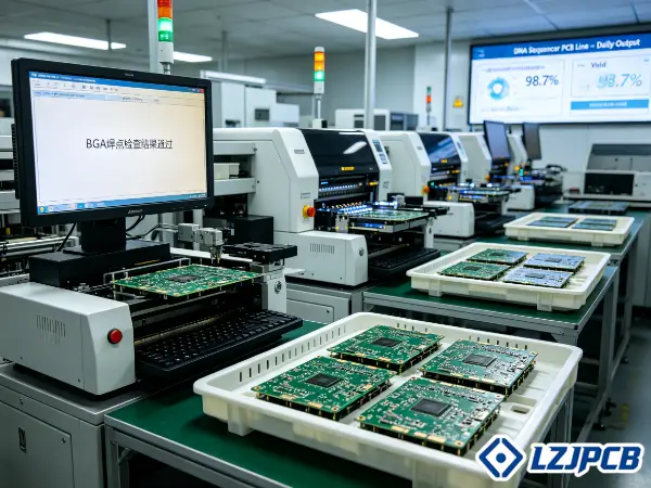
5 Critical Quality Tests for Medical PCB Assembly in DNA Sequencers
A hidden defect can pass a quick look, Then it fails in the field during a patient sample. That risk is not acceptable.
The five critical quality tests for DNA sequencer PCB assembly are electrical continuity and isolation testing, impedance control testing, thermal cycling, X-ray inspection for BGA and microvia joints, and cleanliness testing. Together they catch defects before the board reaches your lab.
I run advanced inspection and test coverage on every medical PCB board. This includes AOI, ICT, flying probe, and functional testing. Let me detail the five tests that matter most.
Electrical Testing: Continuity and Isolation Verification
Electrical testing is the first gate, It confirms every net connects correctly and stays isolated where needed.
I run 100% electrical test on each board. Continuity checks that signals reach their targets. Isolation checks that nets do not short to neighbors. For assembled boards, I add ICT and flying probe testing to verify each component and net. The rule for medical boards is simple: zero defects accepted.
A clean electrical test means the basic wiring is sound. Only then does the deeper testing make sense.
Impedance Control Testing for High-Frequency Signal Integrity
A sequencer moves fast data between sensors and processors. Impedance must stay within tight limits or signals reflect and corrupt.
I verify impedance with TDR measurement per IPC-TM-650. The target is ±5% tolerance for both single-ended and differential lines. For very high-speed channels, I also run insertion and return loss testing up to 50GHz. The goal is insertion loss at or below 0.58dB at 50GHz for reliable transfer.
Controlled impedance keeps the eye diagram open. An open eye means low bit errors and reliable sequencing data.
Thermal Cycling Tests for Operational Reliability
A medical device runs for years. It heats and cools many times. Solder joints and microvias must survive that stress.
I run thermal cycling from -40°C to 125°C for 1000 cycles. Some builds need a wider range, such as -55°C to 125°C, to verify joint and microvia strength. This test exposes weak joints before the board ships, It proves the board will hold through real lab use over a 5 to 15-year life.
Thermal cycling is how I prove long-term reliability. A board that survives the chamber survives the field.
X-Ray Inspection for BGA and Microvia Solder Joint Integrity
Many joints hide under BGAs and inside microvias, You cannot see them by eye. X-ray is the only way to confirm them.
I use X-ray inspection to check hidden joints under BGAs and QFNs. It finds voids, bridges, and weak fills. I also use microvia cross-section analysis to detect plating voids. This matters because stacked or poorly plated vias add parasitics and fail over time.
X-ray catches what AOI cannot reach. For dense HDI sequencer boards, this step is not optional.
Cleanliness Testing for Medical-Grade Contamination Control
Residue on a board causes leakage and migration. In a sequencer near the sample handling, that risk grows. Clean boards are medical-grade boards.
I enforce strict ionic contamination control during assembly. This stops leakage paths and dendrite growth. Medical assembly runs in controlled cleanrooms with HEPA-filtered air and ESD-safe stations. I test ionic cleanliness to confirm residue stays within limits.
Cleanliness testing protects both the signal and the patient sample. It is the final guard against slow, hidden failure.
How Much Does Medical PCB Assembly for DNA Sequencers Cost
You want a fair price, also fear hidden costs from rework and failure. Both fears are real in medical work.
Medical PCB assembly cost for DNA sequencers depends on four drivers: layer count and HDI complexity, material grade and surface finish, order quantity versus MOQ, and assembly complexity. Higher layers, premium materials, and dense assembly raise the cost the most.
I give clients clear cost breakdowns, No surprises. Let me show the four main drivers so you can plan your budget.
Layer Count and HDI Complexity Impact on Manufacturing Cost
Layer count is the biggest cost driver. Each layer adds material, process steps, and test time.
A sequencer board often runs 6 to 18 layers. Imaging boards can exceed 20 layers. HDI adds more cost through laser drilling and tight registration. Higher HDI orders, like 3+N+3, cost more than a single 1+N+1 build. Microvia plating and ±25μm registration also add process control cost.
Here is the rough cost trend:
- 4-6 layers: lower cost, simple builds
- 8-14 layers with HDI: medium cost, most sequencer boards
- 16+ layers with high-order HDI: high cost, imaging modules
I help clients balance layer count against need. Sometimes a smart stackup cuts a layer and saves cost without hurting signal integrity.
Material Grade and Surface Finish Cost Drivers
Material grade shifts price a lot. Premium laminates cost more but perform better.
Standard FR-4 is the cheapest base. High-Tg FR-4 costs more for heat tolerance. Low-loss and Rogers materials cost the most, and you use them only for high-frequency data acquisition. Surface finish adds cost too. ENIG and ENEPIG cost more than HASL. Hard gold on edge connectors adds plating cost by area.
| Item | Lower Cost | Higher Cost |
|---|---|---|
| Base material | Standard FR-4 | Low-loss, Rogers |
| Surface finish | HASL, OSP | ENEPIG, hard gold |
I match the material to the real need. You should not pay for Rogers on a board that runs slow signals.
MOQ Considerations for Prototype vs Production Quantities
Quantity changes your per-board price, the setup cost spreads over the run.
Prototypes cost more per board because setup dominates. Production runs lower the unit price as volume grows. At LZJPCB we support prototyping with no minimum order quantity, so you can validate the design first. We kit samples as fast as 3 days and scale to mass production when you are ready.
My advice on quantity:
- Prototype: small batch, validate design and signal integrity
- Pilot run: confirm yield and assembly process
- Production: scale up for lower unit cost
A clean prototype to production path avoids waste. You only scale a design you trust.
Assembly Complexity: SMT vs Through-Hole Component Placement
Assembly type affects both cost and reliability. SMT and through-hole serve different roles.
SMT dominates sequencer boards. It places parts down to 01005 and 0.35mm pitch BGA with high accuracy. SMT is fast and automated, so cost stays controlled at volume. Through-hole costs more per joint because it needs wave or hand soldering. You still need it for strong connectors and large capacitors. Mixed assembly raises cost because the board passes through more process steps.
I plan the assembly flow to protect heat-sensitive parts. Good sequencing of SMT and through-hole keeps quality high and cost fair.
How to Verify a Medical PCB Manufacturer for DNA Sequencer Production
A wrong supplier hurts you twice. First with bad boards, then with no records when an auditor asks. Verify before you commit.
Verify a medical PCB manufacturer by confirming ISO 13485 and FDA registration, checking traceability and serialization systems, auditing cleanroom and contamination controls, and asking targeted questions before your first order. Proof matters more than promises.
I tell buyers to treat verification like an audit. Ask for documents, visit the floor if you can. Let me give you the checklist I use.
ISO 13485 and FDA Registration Verification Process
Certification is the entry point. Without it, the conversation stops.
ISO 13485 is non-negotiable for medical devices. Ask for the current certificate and check the scope and expiry date. For the US market, the maker should hold FDA establishment registration. You can verify registration in the FDA database. Also confirm IPC Class 3 capability through certificates and references.
I prefer makers with proven medical-device experience, especially in DNA analytics or similar diagnostic systems. A real track record beats a fresh certificate.
Traceability Systems: Serialization and Lot Tracking Requirements
Traceability is the backbone of medical compliance. You must reconstruct how any board was made.
The maker should track every material lot, process parameter, and inspection result. Ask about serialization and lot tracking on each board. Strong suppliers support full Device History Record documentation for regulatory needs, They also provide material certification and process records.
I require strong documentation, revision control, and BOM traceability from prototype through production. This discipline saves you during an audit or a field issue.
Cleanroom Manufacturing Capabilities and Contamination Controls
Clean manufacturing protects sequencer electronics, sample-handling zones make this even more important.
Medical assembly should run in ISO Class 7 or Class 8 cleanrooms, with Class 6 for higher-risk work. The floor needs HEPA-filtered air, ESD-protected stations, and gowning rules. Strict ionic contamination control stops leakage and migration. At LZJPCB, our FPC factory runs a Class 100K cleanroom, and our medical lines hold ISO 13485 certification.
I verify both contamination control and ESD-safe handling. Medical research devices fail from both contamination and static damage.
Questions to Ask Before Placing Your First Order
The right questions reveal the truth fast. Vague answers are a warning sign.
Here are the questions I tell every buyer to ask:
- What is your documented yield rate for Class 3 medical boards?
- How do you handle component traceability and lot tracking?
- How do you manage engineering changes mid-production?
- Can you show references from similar DNA analytics or diagnostic programs?
- What is your procedure for obsolete components?
- Do you offer DFM and DFT review at design stage?
I value a partner who acts as an engineering collaborator. Early DFM and signal integrity feedback cuts validation cycles and raises sequencer reliability.
Customization Options for Medical PCB Assembly in DNA Sequencers
A generic board rarely fits a sequencer. Tight space, lab exposure, and special signals demand custom work. Standard catalog boards fall short.
Customization options for DNA sequencer PCBs include rigid-flex hybrid designs for tight layouts, conformal coating for moisture and reagent protection, custom layer stackups for specific signal needs, and managed lead time from prototype to production. Custom builds match the real device.
I treat each sequencer as a unique problem. The board must fit the housing, survive the lab, and protect the signals. Let me show the main custom paths.
Rigid-Flex Hybrid Designs for Space-Constrained Sequencer Layouts
Sequencers pack parts into small housings. Connectors and cables waste space and add failure points. Rigid-flex solves this.
Rigid-flex combines stable rigid sections with bending flex sections. It removes connectors and fits irregular spaces. This lowers the failure count and saves room. At LZJPCB, we build rigid-flex from 4 to 14 layers, with flex thickness from 0.06mm and rigid-flex up to 6.0mm. We have shipped rigid-flex boards for medical device controllers.
I use rigid-flex when the sequencer layout is tight or folds. Fewer connectors mean higher reliability over the device life.
Conformal Coating Options for Moisture and Reagent Protection
A sequencer sits near reagents and samples, Moisture and chemicals attack exposed boards. Coating builds a barrier.
If the board sits near sample-handling areas, I add conformal coating. Common options protect against moisture and reagents. Parylene coatings give an excellent biocompatible barrier. The coating must resist the lab chemistry and any sterilization the device faces.
Here is how I match coating to risk:
- Light moisture exposure: acrylic or urethane coating
- Reagent and chemical exposure: parylene barrier
- Sterilization exposure: verify coating survives the cycle
I always ask where the board sits. A coating choice depends on the real exposure near the board.
Custom Layer Stackups for Specific Sequencing Application Needs
Every sequencing application has its own signal mix. A custom stackup tunes the board to that mix.
I design stackups to nest signal layers between solid ground planes. A symmetric build keeps warpage under 0.2mm/m and stabilizes impedance. For high-speed sections, I use a 2+N+2 HDI structure with tight dielectric spacing. For imaging modules, I plan isolated power and low-noise analog zones.
A custom stackup protects weak signals and controls heat. It is where signal integrity and reliability come together for the sequencer.
Lead Time and Prototype to Production Transition Planning
Long lead time slows your launch. A weak transition plan breaks quality at scale. Both hurt your market timing.
I plan the path from prototype to production early. Prototype builds validate the design and signal integrity first. At LZJPCB, our PCB lead time runs as fast as 12 hours for single and double-sided, 24 hours for 4-layer, and 48 hours for 6-layer expedited, with 99%+ on-time delivery. PCBA can start as fast as 8 hours, and kitted material goes online within 2 hours.
Here is the transition flow I recommend:
- Prototype: validate design, run DFM and signal integrity review
- Pilot: confirm yield and assembly process
- Production: scale with stable documentation and traceability
A planned transition keeps quality steady as volume grows. You protect both speed and reliability.
4 Common Pitfalls to Avoid in DNA Sequencers PCB Assembly
Small mistakes feel cheap at first. Then they cost you a failed run, a missed approval, or a recall. The pain comes later, and it comes hard.
The four common pitfalls in DNA sequencer PCB assembly are underestimating signal integrity for sensor data, overlooking cleanliness standards, ignoring long-term reliability testing for medical approvals, and inadequate component sourcing for medical certifications. Each one risks data, time, and compliance.
I have seen each of these pitfalls sink a project. The good news is they are all avoidable. Let me walk through the four and how to dodge them.
Underestimating Signal Integrity Requirements for Sensor Data
Teams often treat sensor signals like normal signals, they are not. Weak fluorescence and optical signals need protection.
The fix is to plan signal integrity from the start. Use controlled impedance at ±5%. Separate analog and digital sections. Add a multi-ground architecture and shielding for weak detection circuits. Keep return paths short and reference planes solid. Skipping these steps adds crosstalk and noise that corrupt the read.
I prioritize ultra-low noise design for every sequencer. The sensor data is the whole point of the machine.
Overlooking Cleanliness Standards in Assembly Environments
Some assemblers skip strict cleanliness to save time. The residue stays hidden, then causes leakage later.
The fix is strict contamination control. Run assembly in a controlled cleanroom with HEPA air and ESD-safe stations. Enforce ionic contamination control and test for residue. Near sample-handling areas, this matters even more. A clean board avoids leakage paths and slow failure.
I never trade cleanliness for speed on a medical board. The hidden cost of residue is far higher than the saved time.
Ignoring Long-Term Reliability Testing for Medical Approvals
Teams rush to ship and skip reliability testing, then the device fails an approval or fails in the field years later.
The fix is to test for the full life. Run thermal cycling from -40°C to 125°C for 1000 cycles. Add environmental stress screening for life-sustaining roles. Verify the board holds across a 5 to 15-year service life. Document every result for the regulatory file.
I treat reliability testing as proof, not paperwork. Medical approvals depend on this evidence.
Inadequate Component Sourcing for Medical-Grade Certifications
Cheap or gray-market parts look fine on a BOM, then they fail certification or carry no traceability.
The fix is sourcing from original makers and tier-1 agents only. Demand 100% genuine and traceable parts with IQC inspection. Keep full BOM traceability and material certification, Plan for obsolete parts early. Turnkey assembly helps here because sourcing, soldering, and testing stay under one quality system.
At LZJPCB, our supply chain team sources from TI, ADI, ST, NXP, and other trusted makers, with FIFO and ESD-safe warehousing. Turnkey is often the safest path for a sequencer program.
Conclusion
Choose a medical PCB partner with ISO 13485, IPC Class 3, HDI capability, full traceability, and proven signal integrity. LZJPCB delivers turnkey DNA sequencer boards from prototype to production.