Skip to content
The SMT assembly process runs through 10 stages: solder paste printing, solder paste inspection, component placement, pre-reflow AOI, reflow soldering, post-reflow AOI, X-ray inspection, in-circuit testing, functional testing, and cleaning with conformal coating.Each stage catches defects before they reach the next.
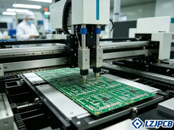
I have run more than 300 PCB projects. The factories that win keep every one of these stages tight. Let me walk you through each one, the way I explain it to my own clients.
What Is the SMT Assembly Process?
Your product needs to be small, light, and cheap to build. Through-hole boards cannot get you there. SMT is the answer that changed the whole industry.
**The SMT assembly process places and solders components directly onto pads on the surface of the PCB. Surface Mount Technology was developed to reduce manufacturing costs and use board space more efficiently than through-hole assembly. Higher automation gives you complex circuits in smaller sizes with good repeatability.
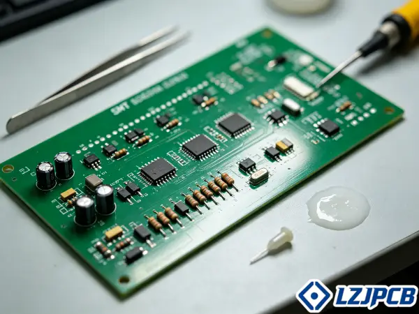
SMT is now the dominant way to build compact electronics. The reason is simple. Smaller parts allow finer circuit designs and smaller finished products. I see this every day in the medical and automotive boards my team builds.
How SMT Differs From Through-Hole Assembly
The core difference sits in how the component meets the board. Through-hole technology uses drilled holes. Leads pass through the hole and get soldered on the other side. SMT skips the holes. Components sit flat on surface pads and get soldered right there.
This one change drives everything else. Surface-mount devices, or SMDs, reduce size and weight by 60% to 90% compared to their through-hole counterparts. The best cases reach one-tenth of the old size. That is a huge saving on space and material.
Here is a simple view of the two:
| Point | SMT | Through-Hole |
|---|---|---|
| Mounting | Pads on the surface | Drilled holes |
| Part size | 60%–90% smaller | Larger |
| Automation | Very high | Lower |
| Density | Fine, high | Coarse |
| Best use | Compact electronics | High-stress, high-power parts |
Many boards still need both. Long-lead parts or high-power connectors often go through-hole after the SMT process finishes. I plan this mix during design, so nothing fights for space later.
What You Need Before the Process Starts
Before SMT assembly starts, you need three things: the PCB, the correct data files to program the machines, and the components in machine-friendly packaging. You also need a stencil and solder paste ready. The SMT process really begins at the design phase, when parts are chosen and the board is laid out.
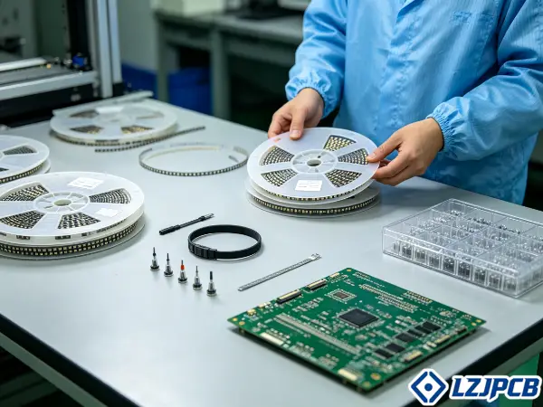
I always tell clients to think about Design for Manufacture and Assembly early. DFMA choices made during layout affect cost and yield later. Good prep saves labor and shortens lead time.
Files Required to Program SMT Machines
Placement machines and AOI systems both need a program. The best source is CAD data. From CAD we pull the centroid file, also called the placement or XY file. This file tells the machine where each part sits.
Quite often CAD data is not available. That is fine. Gerber data is almost always there, because it is the same data used to make the bare board. We can work from Gerber instead.
There is a trade-off though. Using Gerber is less efficient. We have to extract the placement data indirectly, since Gerber was never built to carry centroid points. This adds time to programming.
The workflow looks like this:
- CAD data available: pull centroid file directly, fast and clean.
- Only Gerber available: view the Gerber, extract placement data, program the machine.
- Panel design set before fabrication: board format matches the machines.
- Surface finish specified early: received boards suit the assembly line.
I push for CAD data whenever a client can send it. It removes guesswork and speeds up the first run.
Stencil and Solder Paste Preparation
Solder paste printing needs a stencil and a squeegee. The stencil is a thin metal sheet with openings that match each pad. For complex assemblies, stencil design is a key success factor. A good stencil gives a repeatable, stable print. A poor one gives defects on board one.
Component packaging matters just as much. Parts come in reels, tubes, or trays. Reels are the format we prefer, because they feed machines cleanly. Tubes and trays need different feeder types. Loose parts in bags should be avoided, since they force hand placement or special feeding plates.
Minimum order quantities often force parts into tubes or short strips instead of reels. When that happens, we plan the feeder setup around it. Tray parts can be converted to tape-and-reel by specialist service providers, following industry standards. I use this when a build needs full automation.
One more rule. Moisture-sensitive parts must be handled to the J-STD-033 standard before use. Skip this and you risk cracking during reflow.
1. Solder Paste Printing
The first stage sets the base for every solder joint. Get the paste wrong and nothing downstream can save it. This is where quality control truly begins.
Solder paste printing applies paste to the PCB pads through the stencil openings. The board halts under the stencil while a squeegee forces paste through the openings onto the pads. It needs precise alignment and pressure control. This is still the most common paste method today.
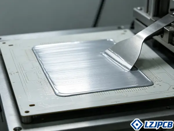
A loader machine feeds bare boards one by one into the printer. Each board advances after the last one clears. Printing defects that slip through will cause defects further down the line, so I treat this stage as critical.
Jet printing is becoming more popular, mostly in the sub-contract sector. It drops paste without a stencil, which makes changes easier. It is not the dominant method yet, but I watch it closely.
How Stencil Thickness Affects Paste Volume
Stencil thickness controls how much paste lands on each pad. A thicker stencil deposits more paste. A thinner stencil deposits less. This is a direct relationship, and it drives joint quality.
Fine-pitch parts need less paste, or you get bridges. Larger parts need more paste for a strong joint. Since one board often carries both, the stencil design must balance them. Sometimes we use a stepped stencil, thicker in some zones and thinner in others.
Here is how I think about it:
- Too much paste: risk of bridging and solder balls between fine pins.
- Too little paste: weak joints, open circuits, poor wetting.
- Correct volume: full, clean joints across all part sizes.
- Complex mix of parts: consider a stepped stencil design.
Paste volume per pad is not a guess. We measure it in the next stage. But the stencil sets the target, so I spend real time on stencil design for tricky boards.
2. Solder Paste Inspection (SPI)
Bad paste hides in plain sight. You cannot judge volume by eye. This gate stops flawed prints before parts ever land.
Solder Paste Inspection captures images of every print and checks four parameters against reference standards: paste position, surface quality, shape, and thickness or volume. It runs before any components are placed. This catches print defects at the earliest possible point.
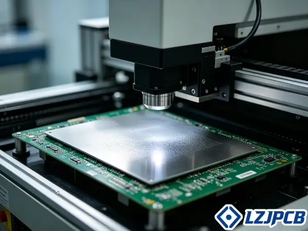
Most paste printers offer a built-in inspection option. That built-in check usually uses 2D technology and measures print area only. For larger boards it also gets slow. So a separate, dedicated SPI machine is often the better choice.
A dedicated SPI machine uses 3D technology. It measures paste volume per pad, not just area. That is a big step up in accuracy. When SPI finds non-conforming paste, my engineers pause the line and fix the root cause before running more boards. SPI is a gating checkpoint.
SPI can also network with the printer. This creates a closed loop. Based on SPI data, the printer adjusts PCB-to-stencil alignment on its own, with no manual step. That kind of feedback keeps a long run stable.
3. Component Placement
Now the board gets its parts. Modern lines place thousands of components per minute. Speed and accuracy must work together here.
Component placement picks each part with a vacuum nozzle or gripper, checks it with a vision system, and sets it at the programmed spot at high speed. Feeders mounted on the machine deliver the parts to the robot arms. A standard line uses at least two placement machines for different part sizes.
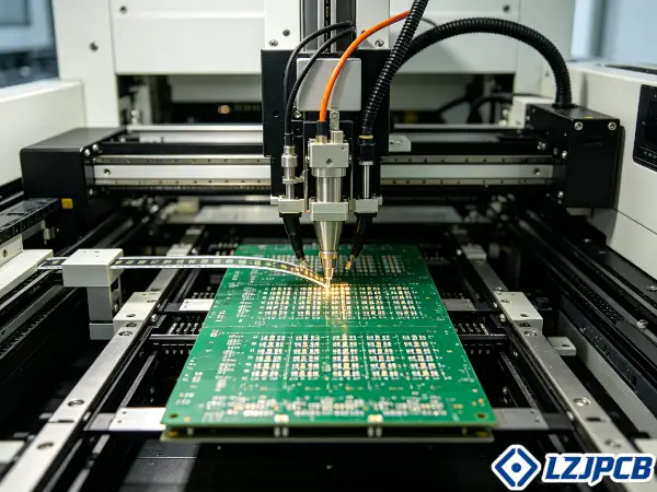
To get accurate, repeatable placement, the board must be fully supported during this stage. A board that flexes gives misplaced parts. I make sure our support systems hold every board flat.
A standard automatic line runs two machine types. One high-speed machine handles small parts like resistors, ceramic capacitors, and inductors. One functional machine handles larger parts like electrolytic capacitors, ICs, and connectors.
How Pick-and-Place Machines Position Components
The sequence is the same for every part. The nozzle picks the component from the feeder. A vision system checks it, confirming the part is correct and centered. Then the arm moves it to the exact XY coordinate on the board and sets it down.
Machine choice depends on your business. If you build large quantities, placement rate matters most. If you run small-batch, high-mix work, flexibility matters most. I match the line to the job, so clients do not pay for the wrong strength.
Placement rate and flexibility trade off like this:
| Focus | Priority | Machine Type |
|---|---|---|
| High volume | Placement speed | High-speed placer |
| Small-batch, high-mix | Fast changeover | Flexible placer |
| Mixed part sizes | Both | Two-machine line |
Placement can also self-correct. When AOI networks back to the placement machine, it adjusts placement positions automatically based on inspection results. That closes another feedback loop.
What First Article Inspection Verifies
First Article Inspection, or FAI, is a critical check for a sub-contract manufacturer. It confirms the first assembly matches the customer specification. Any error missed here can lead to huge volumes of rework. I never skip it.
FAI reads and displays component values on a selected board from the run and checks them against allowed tolerances. The readings are both announced out loud and shown on screen. This dual verification lowers the chance of a missed error.
For prototype projects, we run FAI after the full SMT assembly process completes. If a result is not good, we troubleshoot across the whole prototype project until every issue is solved. We do not just fix the one sampled board. That habit protects the client’s first production run.
4. Pre-Reflow Optical Inspection
Reflow makes solder joints permanent. A wrong part after reflow means costly rework. This stage catches mistakes while they are still cheap.
Pre-reflow AOI verifies component presence, type or value, and polarity before the board enters the reflow oven. It catches placement errors while the paste is still wet and parts can be corrected easily. This step protects against soldering mistakes into place.
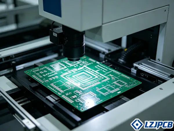
I treat this as a gate. The board moves into reflow only after all placements pass this check. Catching a missing or flipped part here is simple. Catching it after reflow means desoldering, cleaning, and replacing. The math always favors early inspection.
An optical camera scans the board and a computer analyzes the images. At our stations, a dedicated technician also reviews the boards and marks issues. Machine plus human gives strong coverage. This mix has saved many first runs for my clients over the years.
5. Reflow Soldering
This is the moment the board comes alive. Heat turns paste into real electrical connections. The profile decides whether joints are strong or ruined.
Reflow soldering forms all electrical solder connections by heating the assembly to the right temperature. The correct reflow profile is the key. It ensures good joints without damaging parts from too much heat. The board then cools in a controlled way to finish the PCBA.

Reflow ovens usually have 8 to 12 temperature zones. They come as standard air or nitrogen atmosphere types. The choice depends on the solder paste and component needs. We pick the oven setup to match each job.
Lead-free soldering makes the profile even more important. The needed reflow temperature often sits very close to many parts’ maximum rated temperature. That small margin means precise profiling matters more than it did with lead-based solder.
How the Reflow Temperature Profile Works
The profile moves through clear phases in order. Each phase has a job:
- Preheat: raise the temperature slowly to avoid thermal shock.
- Soak: hold steady to activate the flux and even out heat across the board.
- Reflow: hit peak temperature, where intermetallic compounds form between solder and pads.
- Cooling: bring the board down in a controlled way to set strong joints.
The reflow phase is where the real bond happens. The intermetallic layer between solder and pad is what makes the joint reliable. Too little heat leaves a weak or open joint. Too much heat damages the parts. The profile walks that line.
Nitrogen ovens are an option for cleaner joints. Standard air ovens work for many builds. I choose based on the paste and the parts. When a client runs sensitive, fine-pitch parts, I lean toward tighter profiling and often nitrogen.
6. Post-Reflow Optical Inspection
Post-reflow AOI inspects solder joint quality after soldering. It checks that joints are complete, parts stayed in place, and nothing shifted during reflow. Newer machines network back to earlier machines for instant feedback, creating closed-loop process control across the line.
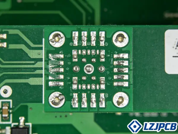
Our in-line AOI uses three-dimensional scanning. 3D gives more comprehensive defect detection than 2D. It also takes more accurate measurements and cuts false calls. 2D systems used to produce high levels of false calls from image interpretation limits. 3D fixed most of that and gives a more stable process.
When AOI finds a bad board, it is separated from the good ones right away and sent for repair. Defective units never move deeper into manufacturing. A technician also reviews and marks issues at each station, on top of the camera and computer.
The networking here is powerful. AOI-to-placement feedback lets the placement machine correct positions on its own. This is one of the newer features, so not every line has it yet. Ours does, and it keeps long runs consistent.
7. X-Ray Inspection
Some joints hide under the part itself. No camera can see them from above. X-ray looks straight through to find hidden faults.
X-ray inspection is a non-destructive way to verify hidden solder joints, including those under BGA components. It also measures voiding inside joints and checks solder hole fill. Because it does not damage the board, we use it for process verification without scrapping assemblies.
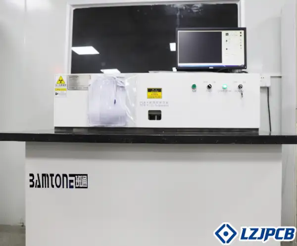
Not every board needs X-ray. We use it when the board carries BGAs or other hidden joints. For simple boards, AOI is enough. But when hidden joints exist, X-ray becomes essential. I add it to the plan the moment I see a BGA on the BOM.
Why BGA Joints Require X-Ray Inspection
A BGA sits on a grid of solder balls under the package. Once placed, those balls are hidden. AOI and human eyes cannot see them. After reflow, the balls melt and form joints you still cannot reach. X-ray is the only practical way to check them.
For BGA boards, X-ray inspection detects hidden defects beneath the component. It checks the solder balls for breaks, pinholes, and other faults after reflow soldering. This runs after reflow, because that is when the balls have melted and set into final joints.
X-ray gives three specific results that other methods cannot:
- BGA joints: confirms every hidden ball formed a good joint.
- Voiding: measures the void percentage inside a joint.
- Hole fill: verifies how well solder filled through-holes.
Voiding matters because too much void weakens a joint and can cause failure later. Hole fill matters for through-hole reliability. I lean on X-ray for high-reliability medical and automotive boards, where a hidden void is not something a client can afford.
8. In-Circuit Testing (ICT)
Good joints do not guarantee good parts. A wrong value or damaged component can still pass a visual check. ICT tests the board electrically.
In-Circuit Testing detects open circuits and short circuits on an assembled board. It also measures passive component values like resistance, capacitance, and inductance to check component integrity. ICT runs after reflow, so it reflects the final assembled state, not the bare board.
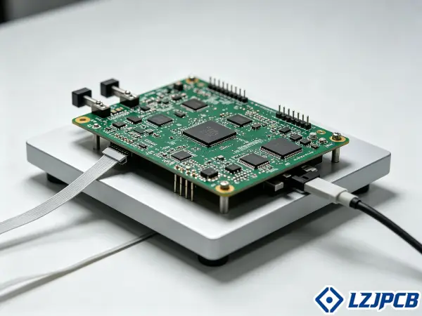
ICT measures values as a proxy for defects. A wrong resistance points to a wrong part. An open reading points to a bad joint. A short points to a solder bridge. These are process defects, not design logic errors. That is exactly what ICT is built to find.
The timing is important. ICT must run after soldering is complete and joints have solidified. Testing before reflow would not reflect the real assembled board. We verify that parts perform to spec in the finished state, which is what clients actually ship.
ICT has a limit worth stating clearly. It validates continuity and component parameters, but it cannot verify how the finished product operates. It checks structure, not behavior. That gap is why the next stage exists. I explain this to every client so they do not treat ICT as the final word.
9. Functional Testing
Functional testing verifies that the assembled board operates correctly under real or simulated operating conditions. It applies power and stimulates inputs, then checks the outputs. It complements ICT rather than replacing it, closing the coverage gap that ICT cannot reach on its own.
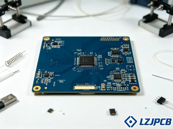
ICT covers structural defects. Functional testing covers operational defects. Neither one alone reaches full fault coverage. The two are complementary by design. This is why I run both on high-reliability boards, targeting different defect classes at different stages.
The order matters. ICT comes first, because functional testing assumes a board free of basic continuity faults. Run functional testing on a board with open joints and the results mean nothing. So the sequence is fixed: fix structure first, then test behavior.
Functional testing usually covers real operation:
- Power-on: confirm the board powers up correctly.
- Signal checks: verify signal integrity where it matters.
- Interfaces: test interaction with external connectors and ports.
- Output validation: confirm the board does its intended job.
Functional testing is the final quality gate before release. The cost of a field failure is far higher than the combined cost of ICT and functional testing. That math is why I never skip it for products going to demanding markets like industrial automation clients.
10. Cleaning and Conformal Coating
The board works, but the job is not done. Flux residue and harsh environments can shorten its life. These last steps protect the finished product.
Cleaning removes contaminants, debris, and flux residues after soldering, even with No-Clean fluxes. Conformal coating then applies a thin polymeric film, usually 25 to 250µm thick, to protect the board from environmental corrosion. Together they extend the working life of the assembly.
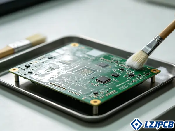
Cleaning is still needed in several cases. It is required when the board needs conformal coating, when aesthetics matter, or when flux residues could create current leakage paths in high-voltage applications. Many companies moved to No-Clean flux, but that does not remove the need to clean in these cases.
Conformal coating conforms to the shape of the board and its parts. It covers solder joints, leads, exposed traces, and other metallized areas all at once. The film reaches irregular surfaces and gets around component features. This is what guards against corrosion over years of use.
Coating is not universal. I apply it only when the board faces environmental exposure, needs high-voltage safety, or must last a long working life. After these steps, the PCBA is a semi-finished product. It may still need IC programming, thermal aging, or box-build assembly. Hand soldering of any leftover fine-pitch or long-lead parts happens here too, as a fallback when automated fitting is not possible.
Common Defects to Avoid During SMT Assembly
Small process errors show up as real defects on the board. Each one has a cause you can control. Knowing them helps you prevent them.
The most common SMT defects are tombstoning, solder bridging, and voiding in solder joints. Most come from paste, placement, or reflow problems. The inspection stages, SPI, AOI, and X-ray, exist to catch each of these before the board ships.
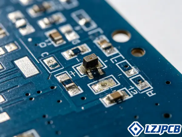
I have seen every one of these across 300-plus projects. The good news is that a tight process with the right inspection catches them early. Let me break down the main ones.
Tombstoning
Tombstoning is when a small two-terminal part stands up on one end, like a tombstone. It happens during reflow when one side of the part heats and wets before the other. The pulling force lifts the far end off the pad.
The usual causes are uneven paste volume, uneven pad heating, or a bad thermal profile. This is why SPI matters, since balanced paste on both pads reduces the risk. A correct reflow profile also keeps heating even across the part.
Solder Bridging
Solder bridging is unwanted solder joining two pads or pins that should stay separate. It creates a short. Fine-pitch parts and too much paste are the common triggers.
SPI catches the excess paste that leads to bridges. AOI and X-ray catch the bridge itself after reflow. A well-designed stencil that meters the right paste volume is the first line of defense. I spend extra care on stencil design for tight-pitch boards for this reason.
Solder Voids
Voids are small gaps of trapped gas inside a solder joint. A little is normal. Too much weakens the joint and can cause failure over time. Voids hide inside the joint, especially under BGAs.
X-ray is the tool that finds and measures them. It gives a void percentage per joint. A good reflow profile and proper paste help keep voids low. For medical and automotive boards, I watch void levels closely, since a hidden void is a hidden risk.
SMT Assembly Process FAQ
The SMT assembly process has 10 core stages, runs on data files and machine-ready parts, and relies on layered inspection to catch defects. Below are the questions I hear most from procurement teams and engineers.
How long does the SMT assembly process take?
Speed depends on the build. At our factory, kitted material can go online within two hours, and we run urgent orders with 7×24 response. Prototype single or double-sided boards ship as fast as 24 hours. Small batches take about 48 hours.
Do double-sided boards need the process twice?
Yes. After the first side finishes AOI, the board returns to the start of the SMT line. The full process repeats on the second side. We plan the paste and reflow for each side so the first side is not damaged when the second runs.
Can one board have both SMT and through-hole parts?
Yes. Many boards mix both. We run SMT first, then handle through-hole parts with selective soldering for longer-lead components. I consider part positioning during design so selective soldering works cleanly.
What files do you need from me?
CAD data is best, since we pull the centroid file directly. If you only have Gerber, we can still work from it, because Gerber is the standard bare-board format. Send a full BOM too, so my supply chain team can source and check every part.
How do I know my board was tested well?
Ask about the inspection stack. A strong line uses SPI, pre-reflow AOI, post-reflow AOI, X-ray for BGAs, ICT, and functional testing. We run 3D AOI and give clients clear inspection records, so you can track quality at every stage.
Conclusion
SMT assembly runs 10 stages, from paste printing to coating. Each inspection gate catches defects early. Tight control at every step is what protects your finished product.