Skip to content
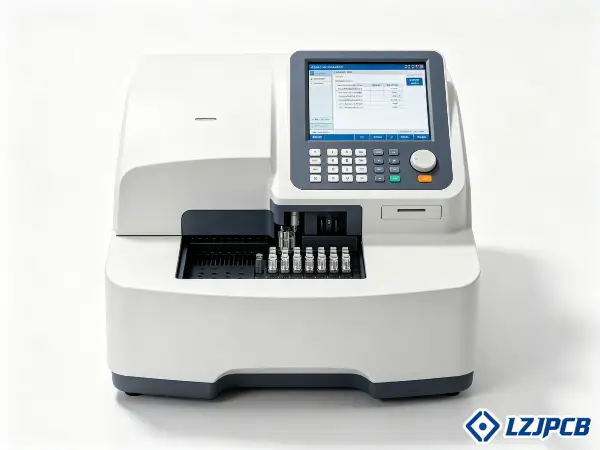
 A faulty PCB can wreck a chemical analyzer’s readings. Sensor drift, noise, and field failures follow. The fix starts with the right board partner.
PCB manufacturing and assembly for a chemical analyzer needs high signal integrity, multilayer builds, IPC Class 3 assembly, ENIG finish, and full testing. These boards process tiny analog sensor signals, so controlled impedance, analog-digital separation, and noise isolation are critical for accurate analysis.
Here is a quick comparison:
| Feature | Standard Industrial PCB | Chemical Analyzer PCB |
|---|---|---|
| Signal level | Volts | Microvolts to millivolts |
| Layer count | 2–4 common | 6–12 common |
| Noise control | Basic | Critical |
| Assembly class | IPC Class 2 | IPC Class 3 |
| Surface finish | HASL often | ENIG preferred |
I have built medical PCB boards with analytical instruments for over seven years. The details below come from real projects. Read on to learn what truly matters before you place an order.
How Chemical Analyzer PCBs Differ from Standard Industrial PCBs
A standard industrial board can handle some noise. A chemical analyzer board cannot. One stray signal can ruin a test result and a customer’s trust.
Chemical analyzer PCBs differ because they process extremely low-level analog signals from sensors and detectors. This forces controlled impedance routing, strict analog-digital separation, multilayer stackups, and tight noise control. Standard industrial boards rarely need this level of precision.
I want to break this down so you can see the real gap. A chemical analyzer reads signals that are often near the noise floor. That changes every design choice.
Defining the PCB Assembly Process for Chemical Analysis Equipment
The assembly process for chemical analysis equipment starts long before the first part is placed. I review the stackup, the BOM, and the test plan first. Then I confirm the board can hold tight impedance and keep analog signals clean. Solder paste printing comes next, with 3D SPI checking every pad. After placement, the board goes through reflow with a tuned profile. I keep the heat steady so fine-pitch parts and BGAs sit right. Inspection follows with AOI and X-ray. For analyzer boards, I also run ICT and functional tests. This catches weak joints and bad parts early. The whole flow stays under Class 3 rules because lab instruments cannot fail in the field. Each step has a record, so you can trace any board back to its materials and process. This level of control is what separates analyzer assembly from basic board work.
The Role of PCB Quality in Analytical Instrument Accuracy
Board quality directly drives how accurately your analyzer reads. A small flaw can shift a result by a wide margin. I have seen a single weak solder joint cause slow sensor drift that took weeks to trace. That is why I push for high standards from the start. Clean copper, stable dielectric, and tight impedance keep the signal true. Good ground planes block stray noise. Strong thermal management keeps readings steady when the board heats up. Thermal vias, copper pours, and smart part placement all help here. When the board is built right, the sensor signal reaches the ADC without loss or noise. When it is built poorly, the instrument lies to the user. For a lab or medical device, that is not an option. So quality is not a nice extra, it is the core of accurate analysis. I treat every analyzer board as a precision tool, not just a circuit.
Chemical Analyzer PCB Types and Material Selection Guide
Pick the wrong material and your board fails in the field. Humidity, voltage, and chemicals all attack weak choices. The right material saves you from costly recalls.
Chemical analyzer PCBs use rigid, flexible, or rigid-flex builds based on layout needs. High-frequency laminates protect sensor signals, chemical-resistant solder masks and ENIG finishes resist corrosion, and high-CTI materials handle high-voltage modules. Material choice depends on signal speed, voltage, and exposure.
Material is where many projects go wrong. I help clients match the board to the real working conditions. Here is how I think through each choice.
Rigid vs Flexible PCBs for Chemical Analyzer Applications
Rigid boards work best for the main control and sensing circuits. They hold parts firmly and support many layers. Flexible boards fit tight spaces and link moving or folded sections. Rigid-flex combines both in one build. I use rigid-flex when the analyzer has a compact body or needs to bend around a sensor head. This cuts connectors, which cuts failure points. Fewer connectors mean fewer spots for noise or corrosion to creep in.
| Type | Best Use | Strength | Watch Out For |
|---|---|---|---|
| Rigid | Main board, dense parts | Stable, many layers | Cannot bend |
| Flexible | Tight or moving links | Light, foldable | Lower part density |
| Rigid-Flex | Compact analyzers | Fewer connectors | Higher build cost |
I pick based on the body shape and the signal path. For most lab analyzers, a rigid main board with a flex link works well. It keeps the signal clean and the build reliable.
High-Frequency Laminate Materials for Sensor Signal Integrity
Sensor signals in an analyzer are weak and fast. They need a stable dielectric to stay clean. Standard FR4 shifts its properties with frequency and heat. That hurts signal integrity. So for high-speed or sensitive paths, I move to Rogers, PTFE, or other low-loss laminates. These hold a steady dielectric constant. That keeps impedance tight and loss low. I have used Rogers ENIG boards for high-frequency analyzer sections with good results. The choice depends on the signal speed and the sensor type. For pure analog low-level signals, the key is low loss and stable Dk. For mixed builds, I sometimes use a hybrid stackup. This puts the fast layers on high-frequency material and the rest on FR4. That controls cost while protecting the signal. The goal stays the same. The signal must reach the chip without drift or distortion. Good laminate choice is the base for that.
Chemical-Resistant Solder Masks and Surface Finishes
Analyzers often sit near fumes, liquids, or high humidity. The board surface must resist that. A weak solder mask will lift or crack, and corrosion follows. So I pick masks rated for chemical contact. For the finish, ENIG is my first choice for analyzer boards. It gives flat pads, great solderability, and strong corrosion resistance. That matters for fine-pitch parts and long service life. If the board faces real chemical or moisture exposure, I add conformal coating on top. This seals the board against the environment. I always raise coating options early, because adding it later means rework. The mask and finish together form the board’s armor. Get them right and the board lasts for years in a harsh lab setting.
CTI Ratings and Dielectric Properties for High-Voltage Modules
Some analyzer sections run at high voltage. Detectors and excitation circuits often need it. High voltage across a board can cause tracking, which is a slow carbon path that shorts the board. The CTI rating measures how well a material resists this. A higher CTI means safer high-voltage spacing. So for high-voltage modules, I pick laminates with a strong CTI rating. I also set wider creepage and clearance in the layout. The dielectric strength of the material matters too. It must hold the voltage without breakdown. I match the material grade to the voltage level on each module. This keeps the board safe and stable over its full life. For medical analyzers, this also helps meet safety standards like IEC 60601-1. Material data sheets list CTI and dielectric values, and I check them before quoting.
How to Choose a PCB Manufacturer for Chemical Analyzer Production
The wrong supplier ships boards that pass their test but fail yours. Lost time and trust follow. The right partner acts like part of your team.
Choose a PCB manufacturer for chemical analyzers with proven medical or analytical-instrument experience, strong process control, and multilayer high-reliability capability. Verify ISO 13485, IEC 60601-1 relevance, and RoHS compliance. The best partners offer engineering support, not just a website order form.
I have sat on both sides of this. I know what a buyer should ask and what a real factory should answer. Here is my checklist.
6 Qualification Questions to Ask Your PCB Assembly Partner
Ask these six questions before you commit. They reveal if the partner can truly handle analyzer boards.
| # | Question | Why It Matters |
|---|---|---|
| 1 | Do you support multilayer 6–12 layer builds? | Analyzers need complex routing |
| 2 | Can you provide ENIG finish? | Needed for solderability and corrosion |
| 3 | Do you run AOI, X-ray, ICT, and functional test? | Catches hidden defects |
| 4 | Can you offer conformal coating? | Protects against humidity and chemicals |
| 5 | What is your IPC class capability? | Class 3 is standard for analyzers |
| 6 | Do you support documentation and traceability? | Required for regulated devices |
If a supplier dodges any of these, walk away. A strong partner answers each one clearly and backs it with proof. I always give a straight answer, because hiding gaps only hurts the project later. These questions filter out the order-platform shops from real instrument-grade factories.
Evaluating Manufacturer Experience with Regulated Medical-Analytical Devices
Experience in regulated devices is not a nice extra. It is a must. Analyzers often fall under medical or lab rules. A factory new to this will miss key steps. I look for a track record with medical and analytical clients. I check for ISO 13485 for medical devices. I confirm the factory understands IEC 60601-1 relevance for safety. I also verify RoHS and REACH compliance. A factory with this background knows how to document, trace, and control every build. They keep records that survive an audit. They also know how to handle change control, which matters when you scale from prototype to production. At LZJPCB, we serve healthcare, industrial automation, and precision electronics, and we hold ISO 13485, ISO 9001, and IATF 16949. That base lets us support analyzer projects from design through mass production. Ask for client examples and certificates. Real experience shows up in the paperwork and the questions the factory asks you.
On-Site Audit Checklist for Chemical Analyzer PCB Facilities
An on-site audit tells you what a sales call cannot. I welcome buyers to visit our floor. When you audit a facility, check these points. First, look at the SMT line. Confirm 3D SPI, inline AOI, and X-ray are in use, not just on paper. Second, check the ESD controls. Analyzer parts are sensitive. Third, review the incoming QC area for component checks. Fourth, ask to see the test stations for ICT and functional test. Fifth, look at the warehouse for FIFO and humidity control. Sixth, review the document system for traceability. Seventh, watch how they handle a defect. A good factory stops the line and records the issue. I also suggest you check the cleanroom for FPC work if your analyzer uses flex boards. An audit takes a day but saves months of trouble. If you cannot visit, ask for a live video walk-through. A confident factory will say yes.
PCB Manufacturing and Assembly Cost Structure for Chemical Analyzers
A low quote can hide a high cost. Cheap material and skipped tests come back to bite you. Smart buyers read the full cost picture.
The cost of a chemical analyzer PCB depends on material grade, layer count, blind vias, volume, and tooling. Chemical-resistant materials and high layer counts raise unit price. NRE and tooling charges apply to complex boards. Prototypes cost more per unit than mass production.
I always give clients a clear cost breakdown. No hidden markups. Here is what drives the price on an analyzer board.
Material Grade Premiums for Chemical-Resistant PCBs
Material is a big cost driver. Standard FR4 is cheap. But analyzer boards often need more. High-frequency laminates like Rogers or PTFE cost much more than FR4. High-TG and high-CTI materials also add cost. Chemical-resistant masks and ENIG finish raise the price too. The premium is real, but it buys reliability. I help clients spend only where it counts. For example, I may use a hybrid stackup. The fast or sensitive layers use premium material. The rest use FR4. This cuts costs without hurting performance. I always explain why each material is needed. If a cheaper option works, I say so. The goal is the right material for the job, not the most expensive one. A clear material plan keeps the budget honest and the board reliable.
Layer Count and Blind Via Impact on Assembly Pricing
Layer count drives both fab and assembly cost. Analyzer boards often need 6 to 12 layers. More layers mean more process steps and higher price. Blind and buried vias add even more. They need extra drilling and lamination cycles. HDI builds with stacked vias cost the most.
| Feature | Cost Impact | When Needed |
|---|---|---|
| 6–8 layers | Moderate | Most analyzers |
| 10–12 layers | Higher | Dense, high-speed boards |
| Blind/buried vias | Adds 15–30% | Tight routing, HDI |
| Stacked microvias | High | Very dense BGA areas |
I push for the lowest layer count that still meets the signal and power needs. Sometimes a smart stackup avoids extra layers, which saves real money. But I never cut layers if it hurts noise control or impedance. The board must work first. Then we optimize cost.
Prototype vs Mass Production Unit Cost Breakdown
Prototype boards always cost more per unit. The setup, tooling, and small batch size drive that. A prototype run of five boards spreads fixed cost over few units. So each one is pricey. Mass production spreads that same cost over thousands. The unit price drops sharply. I tell clients to expect this. The prototype phase is about proving the design, not saving money. Once the design is locked, we move to volume and the price falls. At LZJPCB we support both. We run fast prototypes to validate the board. Then we scale to mass production with the same quality. This path lets you test cheaply on risk and save on volume. I always quote both stages up front so there are no surprises. Planning the jump from prototype to production early also helps lock in component supply and avoid delays.
NRE and Tooling Charges Specific to Complex Analyzer Boards
NRE means non-recurring engineering. It is a one-time charge for setup work. Complex analyzer boards carry higher NRE. This covers stencil making, test fixture build, and program setup. ICT and functional test fixtures cost the most. They are custom to your board. Tooling charges cover drill programs and panel setup. These charges hit hardest at prototype and first production. They spread out over the full run, so high volume softens the impact. I always list NRE and tooling as separate lines. That way you see exactly what you pay for. Some shops hide these in the unit price. I do not. A clear NRE line lets you plan your budget. For a one-time or low-volume build, NRE can be a big share of the cost. For high volume, it fades fast. I help clients balance fixture cost against test coverage so you only build the fixtures you truly need.
Quality Control Standards for Chemical Analyzer PCB Assembly
A board that skips proper testing is a time bomb. It works on the bench, then fails in the lab. Good QC stops that before shipment.
Chemical analyzer PCB assembly should meet IPC-A-610 Class 3 standards. Mandatory checks include electrical test, AOI, X-ray, ICT, and functional test. Thermal cycling, humidity exposure, and ionic contamination testing validate long-term reliability in lab environments.
Quality control is where I never cut corners. For analyzer boards, the bar is high. Here is the full QC picture I follow.
IPC Class 3 vs Class 2 Requirements for Analytical Instruments
IPC sets the rules for assembly quality. Class 2 fits general electronics. Class 3 fits high-reliability gear like medical and analytical instruments. The gap is real and it matters.
| Factor | Class 2 | Class 3 |
|---|---|---|
| Use case | General products | Critical instruments |
| Solder joint rules | Relaxed | Strict |
| Defect tolerance | Higher | Very low |
| Inspection rigor | Standard | Intensive |
| Best for analyzers | No | Yes |
For a chemical analyzer, I always build to Class 3. The instrument must run for years without failure. Class 3 demands the best solder joints, the tightest checks, and the lowest defect rate. It costs a bit more, but it prevents field failures that cost far more. If a supplier offers only Class 2, they are not right for analyzer work. I make Class 3 the default for these projects.
5 Mandatory Electrical Tests for Chemical Analyzer PCBs
Five tests must run on every analyzer board. Skipping anyone leaves a risk open. First, 100% electrical net test. This finds opens and shorts on the bare board. Second, AOI. This scans for placement and solder defects on the assembled board. Third, X-ray. This checks hidden joints under BGAs and connectors. Fourth, ICT, or in-circuit test. This checks each part for value and function. Fifth, functional test. This runs the board like the real analyzer to confirm it works end-to-end. I run all five on analyzer boards because the cost of a field failure is huge. AOI and X-ray catch build defects. ICT and functional test catch part and circuit faults. Together they form a net that almost nothing slips through. I document each test result for traceability. This record proves the board passed before it left the floor.
Thermal Cycling and Humidity Exposure Validation Methods
Analyzers face temperature swings and damp air. So the board must prove it can take that. Thermal cycling moves the board between hot and cold many times. This stresses the solder joints and vias. A weak joint cracks here, not in the field. Humidity exposure puts the board in a damp chamber. This shows if moisture causes leakage or corrosion. I run these tests during validation, before mass production. They confirm the design and process are sound. For boards with conformal coating, these tests also prove the coating works. I match the test profile to the real working range of the analyzer. If the device runs in a lab at steady temperature, the profile is mild. If it runs in a field unit, the profile is harsh. These tests give both the buyer and me confidence that the board will last its full service life.
Ionic Contamination Testing for Chemically Sensitive Circuits
Ionic contamination is a hidden killer for analyzer boards. Leftover flux or salts on the board surface hold moisture. Over time this causes leakage current. For low-level analog circuits, even tiny leakage shifts the reading. So I run ionic contamination testing on these boards. The test measures the ionic residue on the surface. A clean board passes a tight limit. A dirty board fails. If a board fails, I clean and retest it. This step matters most for sensitive sensing circuits where signals are near the noise floor. A clean board keeps the signal true and the sensor stable. I treat this as a standard step for chemically sensitive builds. It is easy to skip and costly to ignore. Clean assembly plus this test keeps drift out of your analyzer.
Chemical Analyzer PCB Customization and Design for Manufacturability
A great design that cannot be built is worthless. Bad design rules cause low yield and high cost. Smart DFM fixes this before fab starts.
Chemical analyzer PCB customization needs design rule changes for microfluidic and sensor interfaces, smart panelization for high-mix low-volume runs, and long-term component sourcing. Strong DFM and DFT review raises yield and cuts cost by catching issues before production.
Custom analyzer boards need real engineering support. This is where our dedicated engineers add the most value. Here is how I approach it.
Design Rule Modifications for Microfluidic and Sensor Interfaces
Analyzer boards often touch fluids and sensors. These spots need special design rules. Near a microfluidic channel, I adjust spacing and add sealing zones. I keep traces away from wet areas. For sensor interfaces, I protect the analog path. This means guard rings around sensitive nets. It means tight impedance on signal lines. It means a solid ground under the sensor pads. I also separate analog and digital sections on the board. Digital switching noise can ruin a weak analog signal. So I split the ground planes and route them apart. This separation is a core rule for analyzer design. I review every interface during DFM. If a rule risks the build or the signal, I flag it early. Fixing it on screen is cheap. Fixing it after fab is not. These custom rules make the difference between a board that reads true and one that drifts.
Panelization and V-Scoring for High-Mix Low-Volume Production
Analyzers often run in small batches with many versions. That is high-mix, low-volume work. Panelization helps here. I group boards on a panel to run them through SMT together. This raises throughput and cuts cost per board. V-scoring cuts a shallow groove so boards snap apart after assembly. It works for straight edges. For complex shapes, I use tab routing instead. The right panel design also protects sensitive edges and parts during depaneling. A bad snap can crack a board near a fine part. So I plan the score lines away from stress points. For high-mix runs, I design flexible panels that fit several board types. This keeps setup low across versions. Good panelization is quiet work, but it saves real money and protects yield on small analyzer batches.
Component Sourcing Strategies for Long-Lifecycle Analyzer Models
Analyzers stay in the market for years. So parts must stay available for years. A part that goes obsolete can stop your whole line. I planned for this from the start. First, I pick parts with long lifecycles from major makers. Second, I list approved alternates in the BOM. If the main part runs short, the alternate steps in. Third, I track supply through our 20-plus supply chain team. We buy from original makers and tier-1 agents only, so parts are genuine and traceable. Fourth, for critical parts, I suggest a buffer stock. This covers gaps during shortages. Our network spans Shenzhen and Indonesia, which gives more sourcing paths. I review the BOM for risk before production. Any single-source or end-of-life part gets flagged early. This planning keeps your analyzer in production without surprise stops. For a long-life product, the sourcing strategy is as important as the design itself.
PCB Assembly Lead Time and Shipping for Chemical Analyzer Orders
A slow supply chain stalls your whole product launch. Late boards mean missed sales and angry customers. Clear lead times and safe shipping prevent that.
Chemical analyzer PCB lead time runs from days for prototypes to two weeks or more for bulk orders. Component delays are the main risk, so buffer stock and alternates help. Moisture-safe, ESD-safe packaging and reliable freight protect boards in transit.
Lead time and shipping worry every buyer I work with. I keep both clear and predictable. Here is what to expect.
Standard Lead Time Ranges for Prototype and Bulk Quantities
Lead time depends on the stage and the build. Prototypes move fast when the design is clean. Bulk orders take longer due to volume and full testing.
| Stage | Typical Lead Time | Notes |
|---|---|---|
| PCB prototype | 24–48 hours | Simple to mid-layer boards |
| PCBA prototype | 24–48 hours | After parts are kitted |
| Small batch | About 48 hours | Once material is ready |
| Bulk production | 1–2 weeks+ | Depends on volume and test |
At LZJPCB, kitted material can go online within 2 hours, and urgent orders get 7×24 response. Our on-time delivery rate stays above 99%. But the real driver of lead time is parts. If parts are in stock, we move fast. If a part has a long lead time, the whole order waits on it. So I confirm part availability before I promise a date. A clear lead time, backed by parts in hand, keeps your launch on track.
Component Procurement Delays and Mitigation Plans
Parts are the top cause of delay. A single long-lead chip can hold a whole board. So I plan around this. First, I check lead times for every part during quoting. Any long-lead part gets flagged. Second, I list alternates so we have a backup. Third, for known risk parts, I suggest buying ahead. This buffer stock covers shortages. Fourth, our supply team tracks the market and buys early when a shortage looms. We source from original makers and tier-1 agents, so we avoid fake parts that cause failures. I keep the client updated if a part slips. No silent delays. If a date moves, you hear it from me with a reason and a plan. This open approach lets you adjust your own schedule. Procurement is where most projects stall, so I treat it as a core part of the job, not an afterthought.
Packaging Requirements to Prevent Moisture and ESD Damage
A board can survive the factory and die in the box. Bad packaging causes that. Analyzer boards hold sensitive parts. They need protection in transit. First, ESD-safe packaging. Static can kill a sensitive analog chip. So we use ESD bags and trays. Second, moisture protection. We seal boards in moisture-barrier bags with desiccant. We add a humidity indicator card. This keeps damp out during shipping and storage. Third, physical protection. We use foam or trays so boards do not knock together. For boards with fine parts or connectors, this matters a lot. I match the packaging to the trip. A long sea route needs more moisture protection than a short flight. Good packaging is cheap insurance. It would be a waste to build a perfect board and lose it to a humid container. So I treat packaging as the last quality step, not a throwaway task.
Freight Options and Customs Clearance for International Shipments
We ship to the USA, Europe, Brazil, Russia, and beyond. Freight choice depends on your speed and budget. Air freight is fast, often a few days, but costs more. Sea freight is cheaper for large or heavy orders, but takes weeks. Express courier suits small urgent shipments with door-to-door service. I help clients pick the right mix. For a launch, air freight gets the first batch there fast. For steady production, sea freight cuts cost. Customs clearance is the other half. We provide correct invoices, HS codes, and documents so your goods clear smoothly. Wrong paperwork causes delays and fees at the border. For European clients like many we serve, we make sure RoHS and REACH documents are ready. This avoids hold-ups in customs. I track the shipment until it lands. A board that ships clean and clears fast keeps your whole timeline intact.
LZJPCB Manufacturing Capabilities for Chemical Analyzers
You need one partner who handles the board, assembly, and parts together. Splitting them across vendors adds risk and delay. One turnkey source fixes that.
LZJPCB supports chemical analyzer projects with turnkey PCB fabrication and PCBA, multilayer builds up to 32 layers in production, component sourcing, ENIG finish, conformal coating, and full testing. Our experience in healthcare, industrial automation, and precision electronics fits analyzer needs.
Let me share what we bring to an analyzer project. We started in 2006 and now run bases in Shenzhen, Ji’an, Changsha, and Indonesia. Our PCB factory builds 1 to 32 layers in mass production, with impedance control at ±5% and ENIG and other finishes. We handle high-frequency boards, HDI, and rigid-flex, all of which analyzers may need. Our PCBA side places parts as small as 01005 with ±0.03mm accuracy on ICs. We run 3D SPI, inline AOI, X-ray, ICT, and functional test. We build to IPC Class 3 for instrument work. Our supply chain team sources genuine, traceable parts and offers full BOM service with no minimum order. We hold ISO 9001, ISO 14001, IATF 16949, ISO 13485, UL, and RoHS. We have built medical MRI control boards, PCR detector control boards, and data acquisition PCBAs, which sit close to analyzer work. Most of all, we give you a dedicated engineer for custom development, not just an order form. That means real DFM and signal integrity support from start to finish.
Why Choose LZJPCB for Chemical Analyzer PCB Supplier
Most factories take your files and hope for the best. When trouble hits, you are alone. You deserve a partner who solves problems with you.
Choose LZJPCB because we act as an engineering partner, not just a factory. We offer 1-on-1 custom support, stackup and signal integrity review, genuine component sourcing, Class 3 assembly, full testing, regulatory documentation, and scalability from prototype to mass production for chemical analyzers.
I will be honest about why I think we fit analyzer work. Many competitors run on website-based ordering. You upload files and wait. If the design has a flaw, no one tells you. We work differently. We assign a dedicated engineer to your project. I and my team review your stackup, your impedance, and your signal paths before we build. We flag risks early. This is the DFM and DFT support that raises yield and cuts cost. For a client named Michael in Germany who buys turnkey boards, this matters. He worries about inconsistent quality, long lead times, and weak after-sales support. We answer each one. We hold tight process control for steady quality. We run multiple bases for faster delivery and flexibility. We track every board for traceability. And we stay reachable after the order ships. The best analyzer supplier gives stackup help, sourcing help, documents, and a clear path from prototype to volume. That is the partner role we play. We sell solutions, not just boards.
Chemical Analyzer PCB Assembly: Common Mistakes and FAQ
Small mistakes in specs cause big failures later. Buyers often learn this the hard way. A quick check now saves a costly redo.
Common chemical analyzer PCB mistakes include wrong surface finish choices and impedance mismatch, which is the top cause of sensor drift. Buyers also ask about MOQ, NRE fees, design file formats, and the Gerber review process. Clear specs up front prevent most problems.
Over many projects, I see the same errors repeat. Let me cover the big ones and answer the questions buyers ask most.
3 Costly Errors in Specifying Surface Finish for Analyzer PCBs
Three finish errors cause real pain. First, picking HASL for fine-pitch parts. HASL leaves uneven pads. Fine-pitch BGAs need flat pads, so ENIG is the right call. Second, skipping corrosion resistance. Analyzers face humidity and fumes. A finish like bare OSP can fail here. ENIG resists corrosion far better. Third, forgetting the finish-to-part match. Some finishes suit some parts poorly. The wrong mix causes weak joints over time.
| Error | Result | Fix |
|---|---|---|
| HASL for fine-pitch | Uneven pads, weak joints | Use ENIG |
| No corrosion plan | Surface fails in humidity | ENIG plus coating |
| Wrong finish-part match | Long-term joint failure | Match finish to parts |
I push ENIG as the default for analyzer boards. It gives flat pads, good solder, and strong corrosion resistance. Get the finish right and you avoid slow, hidden failures.
Why Impedance Mismatch Is the Top Cause of Sensor Drift
Impedance mismatch is the number one cause of sensor drift I see. Here is why. An analyzer sends a weak, fast signal from the sensor to the chip. The trace must hold a set impedance the whole way. If the impedance shifts, the signal reflects and distorts. For a strong digital signal, this may not matter. For a weak analog sensor signal, it ruins the reading. The result is drift that grows over time and is hard to trace. The fix is controlled impedance routing. I set the trace width, spacing, and layer stack to hold the target impedance, often within ±5%. I keep a solid ground plane under the signal. I avoid stubs and sharp turns. I also separate analog and digital so digital noise does not couple in. When the impedance is tight and the signal is clean, the sensor reads true. This is why I review impedance on every analyzer board before fab. It is the single most important signal step.
FAQ: MOQ Policy and Non-Recurring Engineering Fee
Buyers ask about MOQ and NRE often, so let me be clear. On MOQ, we support prototyping with no minimum order quantity. You can order a small batch to prove your design first. This lets you test on low risk before you commit to volume. On NRE, this is a one-time engineering fee for setup. It covers stencils, test fixtures, and program setup. For analyzer boards with ICT and functional test, fixtures drive most of the NRE. We list NRE as a separate line so you see exactly what you pay. For high volume, the NRE spreads thin across units. For one-off or low-volume builds, NRE is a larger share. I always explain both before you order. No hidden fees. If you plan to scale, I help structure the NRE so you do not pay twice. Ask me for a clear quote that splits NRE, tooling, and unit price. That way you can plan your budget with full sight of the costs.
FAQ: Design File Format Requirements and Gerber Review Process
Buyers also ask what files we need and how we review them. For files, we accept Gerber and ODB++ for the board. ODB++ is richer and cuts review time, so I prefer it when you have it. We also need the BOM, the centroid or pick-and-place file, the assembly drawing, the stackup, and your test requirements. For analyzer boards, please also send any contamination or conformal coating needs up front. This lets us confirm feasibility fast. On review, our process is simple. We run a DFM check on your Gerbers first. We look for spacing, impedance, drill, and mask issues. We check the BOM for obsolete or single-source parts. Then I send you a report with any flags and fixes. We do not build until you confirm. This Gerber review catches problems on screen, where fixes are cheap. It is part of our engineering support, not an extra charge. Send complete files and you get a fast, clear feasibility answer.
Conclusion
Chemical analyzer PCBs demand signal integrity, Class 3 assembly, smart materials, and full testing. As your engineering partner, LZJPCB delivers all of it, from prototype to volume.