Skip to content
 Your X-ray machine failed final test. The PCB was the problem. One weak solder joint can stop a hospital diagnosis and risk a patient.
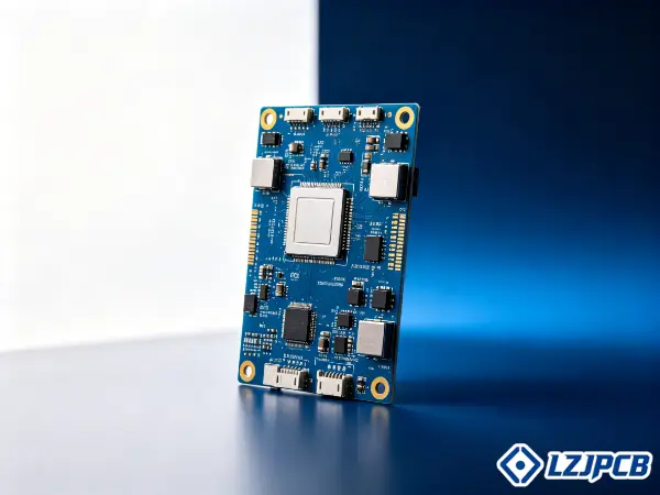
X-ray machine PCBs need specialized manufacturing because they control high-voltage generators, detector signals, and image processing where failure risks patient safety. Build them under ISO 13485 systems, to IPC Class 3 standards, with AOI plus X-ray inspection and full traceability.
I have built boards like these for medical clients across 20+ countries. Let me show you what really matters before you place your order.
Why Do X-ray Medical PCBs Require Specialized Manufacturing
A normal PCB process will not work here. X-ray boards mix high voltage and tiny sensitive signals on one design. That mix breaks weak builds.
X-ray medical PCBs need specialized manufacturing because they combine high-voltage generator control with low-level detector signals on the same board. They support image acquisition, motion control, and diagnostic data, so a single defect can harm a patient or ruin an image.
I split these boards into two worlds. One world pushes high voltage, the other reads weak signals. Both must work on the same build. This is why I never treat an X-ray board like a normal order.
The Unique Electrical Demands of High-Voltage X-ray Generator PCBs
X-ray generators run at very high voltage. The board must stop arcs and slow failures. Two spacing rules matter here: clearance and creepage. Clearance is the air gap between conductors. Creepage is the surface path along the board. If these gaps are too small, the board can arc or fail over time. I follow IEC 60601-1 and IPC-2221 to set these gaps. For a 2xMOPP patient circuit at 300Vrms, I plan around 9mm creepage and 5mm clearance. I also pick the right material. A high CTI value resists surface tracking. Here is how I plan the high-voltage section:
- Confirm the peak voltage between each net.
- Set creepage and clearance from IEC 60601-1 and IPC-2221.
- Add slots or barriers to grow creepage in tight spots.
- Choose a high-CTI, high-Tg, UL 94V-0 base material.
- Use heavy copper for high-current generator traces.
Signal Integrity Requirements for Digital Detector and Image Processing Boards
The detector side is the opposite problem. These signals are weak and fast. Noise here shows up as a bad image. A bad image can hide a real diagnosis. So I protect signal integrity from the start. I use controlled-impedance stackups with a ±5% target. I keep full ground and power planes for clean return paths. I separate the noisy high-voltage zone from the quiet analog zone. Modern digital and AI-assisted imaging runs faster every year, so this matters more now. Here is what I control on the detector and image boards:
- Controlled impedance, often 50–120Ω, held to ±5%.
- Solid ground planes under fast signals.
- Short, matched routing for detector data lines.
- Physical zoning to block EMI from the generator.
- Multilayer or HDI stackups for dense routing.
Key Specifications to Define for Your X-ray Machine PCBs
A vague spec leads to a wrong board. You waste weeks and money. Define the hard numbers before you ask for a quote.
Define material type, layer count and stackup, minimum trace width and spacing, and surface finish before you order. These four specs drive cost, reliability, and signal quality for X-ray machine PCBs, and they let your supplier confirm feasibility fast.
When a client sends me a clear spec, I can quote in a day. When the spec is open, we trade emails for a week. Below are the four areas I always pin down first. Each one changes the build in a real way.
Material Selection for High-Frequency and High-Temperature X-ray Applications
The base material sets the limits of the board. X-ray power sections get hot, so I use high-Tg laminate. The board stays stable under heat. For high-speed detector or imaging signals, I may use Rogers or other high-frequency material. The material also drives the CTI value, which controls creepage limits. Below is a simple guide I use:
| Need | Material Choice | Why |
|---|---|---|
| High-voltage power section | High-Tg FR4, UL 94V-0 | Stays stable and flame-retardant under heat |
| High-speed imaging signals | Rogers / PTFE | Low loss at high frequency |
| Heavy current paths | Heavy copper (up to 12oz) | Lowers temperature rise |
| General control logic | A-grade FR4 (Shengyi, KB) | Reliable and traceable |
I always confirm UL and RoHS traceability on the laminate. Medical clients need that paper trail.
Layer Count and Stack-up Configurations for Complex X-ray Control Boards
Layer count depends on how dense the design is. Simple control boards may need 4 to 6 layers. Complex imaging and control boards often need many more. I have built medical PCB boards up to 22 layers and HDI boards with any-layer interconnects. The stackup is not just about layer count. It places ground planes, power planes, and signal layers in the right order. A good stackup gives clean return paths and low noise. I match the stackup to the job:
- 4–6 layers for basic power and control chassis boards.
- 8–14 layers for mixed control and imaging boards.
- HDI (1+N+1, 2+N+2, 3+N+3) for compact, dense designs.
- Dedicated ground and power planes for low-noise signal chains.
Minimum Trace Width and Spacing for Dense Component Placement
Fine-pitch parts need fine traces. But you cannot shrink everything. High-voltage nets still need wide spacing for safety. So I use two rules on one board. Tight traces in the logic zone, wide gaps in the high-voltage zone. Our process can hold 3/3mil trace and space in mass production, with finer lines in HDI builds. Here is how I balance it:
- Use fine 3/3mil traces only in low-voltage dense areas.
- Keep wide creepage gaps in the high-voltage section.
- Match trace width to current for heavy power lines.
- Confirm BGA pitch support down to 0.3mm for dense ICs.
Surface Finish Options Compatible with Medical-Grade Solder Joint Reliability
The finish protects the pads and shapes the solder joint. For medical work, I lean toward ENIG. It gives flat pads and strong, reliable joints. That helps fine-pitch and BGA parts. Other finishes work for other needs. Here is my quick compare:
| Finish | Best For | Note |
|---|---|---|
| ENIG | Fine-pitch, BGA, medical | Flat, reliable, longer shelf life |
| Immersion silver | High-frequency signals | Good for clean signal paths |
| Lead-free HASL | Simple, low-cost boards | Less flat for fine pitch |
| Electroplated gold | Edge connectors, contacts | Hard, wear-resistant |
For X-ray boards, I almost always pick ENIG or ENIG+OSP for joint reliability.
How to Choose The Right PCBs for X-ray Subsystems
One board type does not fit every part of the machine. The gantry moves. The power chassis sits still. Pick the wrong type and parts crack.
Choose rigid PCBs for stationary power supplies and control chassis, flex circuits for moving gantry arms and collimators, and rigid-flex hybrids for compact C-arm and portable X-ray devices. Match the board type to the mechanical job of each subsystem.
I always ask one question first: does this part move? The answer tells me the board type. A static power box is happy with a rigid board. A moving arm needs flex. A tight portable unit needs rigid-flex. Below I break down each case.
Rigid PCBs for Stationary Power Supplies and Control Chassis
Rigid boards are the base of most X-ray systems. They sit still inside the power supply and the control chassis. They hold heavy parts and high-current traces well. For these I use high-Tg material and often heavy copper. They are strong, stable, and cost-effective. I pick rigid boards when:
- The board is fixed inside a chassis.
- It carries high-voltage or high-current sections.
- It holds heavy or large components.
- Cost and stability matter more than flexibility.
Flex Circuits for Moving Gantry Arms and Collimator Assemblies
Moving parts kill rigid boards over time. Vibration and bending crack the copper. So for gantry arms and collimators I use flex circuits. Flex bends and survives motion. Our FPC factory runs a Class 100K cleanroom and builds 1–8 layer flex down to 2mil traces. We use flex for medical device controllers and similar moving parts. I pick flex when:
- The board must bend or fold during use.
- The part moves or rotates, like a gantry arm.
- Space is tight and a cable plus connector will not fit.
- The design needs to survive repeated motion.
Rigid-Flex Hybrid Boards for Compact C-Arm and Portable X-ray Devices
Sometimes you need both. A C-arm or a portable unit is small and still has moving joints. Rigid-flex gives rigid zones for parts and flex zones for the bends. This removes connectors, saves space, and raises reliability. We build rigid-flex from 8 to 14 layers for medical use. I pick rigid-flex when:
- The device is compact, like a C-arm or portable scanner.
- You need rigid mounting zones and flexible joints together.
- Removing connectors will improve reliability.
- Weight and size are tight limits.
How Much Does X-ray PCB Assembly Cost?
You need a budget number, not a vague range. But X-ray boards have hidden cost drivers. Miss them and your quote jumps later.
X-ray PCB assembly cost depends mostly on board complexity, layer count, and component sourcing. More layers, HDI features, and X-ray-specific materials raise the per-unit price. Genuine traceable components and medical-grade testing add cost but protect patient safety.
I will be honest with clients about cost. There is no single price for an X-ray board. The number moves with layer count, parts, and test needs. But I can show you the main drivers so you can plan. Below I break the cost into two parts: the board itself and the components.
Per-Unit Pricing Breakdown by Board Complexity and Layer Count
The board build is the first cost. Each extra layer adds process steps and price. HDI and heavy copper add more. Tight impedance control adds testing. Volume also matters; prototypes cost more per unit than mass runs. Here is a rough view of what drives the board cost:
- Layer count: more layers mean more cost per unit.
- HDI features: blind and buried vias raise the price.
- Special processes: heavy copper, back drilling, mixed materials.
- Impedance control: ±5% testing adds steps.
- Volume: per-unit cost drops as quantity rises.
Cost Impact of Component Sourcing and X-ray-Specific Material Upcharges
Components often cost more than the bare board. Medical work needs genuine, traceable parts only. I source from original makers and tier-1 agents, never gray market. That protects safety but adds some cost. X-ray-specific materials, like high-Tg laminate and high-CTI substrates, also carry an upcharge. Here is where component and material cost grows:
- Genuine, traceable parts from original makers and tier-1 agents.
- Long-lead or specialty ICs for imaging and control.
- High-Tg and high-CTI material upcharges.
- Heavy copper and Rogers material premiums.
- Medical-grade testing and documentation time.
Turnkey service helps here. When I source the BOM and build the board, I keep one clear cost record and one quality system.
5 Quality Assurance Tests Every X-ray Machine PCB Must Pass Before Shipment
A board that looks fine can still fail in the field. Hidden defects hide under BGAs. In a hospital, that failure is not an option.
Every X-ray machine PCB should pass five tests before shipment: hi-pot and insulation resistance, thermal cycling, conformal coating and creepage checks, X-ray inspection of solder joints, and functional testing with generator or detector simulators. These tests catch hidden and high-voltage defects.
I run these tests because I have seen what happens without them. A hidden void in a BGA can pass a visual check and still fail in service. These five tests catch the defects that matter for X-ray boards. Below I explain each one and why it earns its place.
Electrical Testing: Hi-Pot and Insulation Resistance for High-Voltage Safety
X-ray boards run at high voltage, so I test that insulation holds. A hi-pot test applies a high voltage and checks for breakdown. An insulation resistance test confirms the gaps block current. These tests follow IEC 60601-1. They prove the board is safe for both patient and operator. Without them, a creepage error stays hidden until it arcs in the field.
Thermal Cycling Stress Tests to Validate Performance Under Continuous Operation
X-ray machines run for long hours and heat up. Heat expands and contracts solder joints. Weak joints crack over many cycles. So I run thermal cycling stress tests. The board moves through hot and cold cycles, like real use. Then I retest it. This finds joints that would fail months later. It validates the board for continuous clinical operation.
Conformal Coating Integrity and Creepage Distance Verification
Hospitals clean equipment with chemicals and moisture is common. Both can shorten creepage and cause shorts. A conformal coating protects the board surface. I check the coating for full, even coverage with no gaps over key nets. I also verify the creepage distances match the design and IEC 60601-1. This step protects the board against the hospital environment and contamination.
X-Ray Inspection of Solder Joints and BGA Void Detection
You cannot see under a BGA with your eyes. The joints hide below the package. So I use X-ray inspection. It looks through the part and shows the solder joints. It finds voids, bridges, and missing joints. This is the only reliable way to check hidden, fine-pitch, and BGA joints. We run AOI plus X-ray in the assembly flow for exactly this reason. Here is my inspection chain:
- SPI checks solder paste before placement.
- AOI checks visible joints after reflow.
- X-ray checks hidden BGA and fine-pitch joints.
- Voids and bridges flag the board for rework.
Functional Testing with Actual X-ray Generator or Detector Simulators
The last test is the real one. Does the board actually work in the system, I run functional tests with generator or detector simulators. The board sees signals like the real machine. I also use ICT to check each net. This proves the board performs, not just that it looks right. Documented test records let the client audit and validate the build.
4 Common Mistakes That Delay FDA Clearance for X-ray PCBs
A small board mistake can stall your whole FDA submission. Months of delay. Lost revenue. And the fix is often simple if you plan early.
The four common mistakes that delay FDA clearance for X-ray PCBs are wrong material selection, poor thermal management, ignoring component derating, and missing traceability or documentation. Fix these early in design to keep your 510(k) submission on track.
I have watched good products get stuck at the FDA gate over board-level issues. The hardware was almost right. The paperwork or the margin was not. Here are the four mistakes I see most. Each one is avoidable if you plan it into the design from day one.
Incorrect Material Selection Leading to Dielectric Breakdown Under Load
The wrong material breaks down under high voltage. A low-CTI or low-Tg laminate cannot handle the load. Under stress it tracks, arcs, or fails. That failure stops your safety testing cold. I fix this by choosing high-Tg, high-CTI, UL 94V-0 material from the start. The material must match the operating voltage and the heat. Pick it during design input, not after a failed test.
Inadequate Thermal Management Causing Drift in Image Quality Calibration
Heat is a quiet enemy of image quality. As the board heats, components drift. The image calibration drifts with them. The result is a board that passes cold and fails warm. Modern fast and AI-assisted imaging makes this worse. I manage heat with high-Tg material, heavy copper, planes, and good layout. I add temperature monitoring where the design needs it. Good thermal design keeps calibration stable.
Overlooking Component Derating Specifications for Medical Safety Margins
Medical design needs margin. A part run at its limit may pass test and fail later. Derating means running parts below their max rating. This builds in a safety margin for voltage, current, and temperature. The FDA expects this margin in a Class II device. I check derating during design review and document it. Skipping derating is a common reason a board fails long-term reliability.
Missing Traceability and Documentation Required for 510(k) Submissions
The FDA wants proof, not promises. A 510(k) submission needs design control records, test reports, and full traceability. You must trace every material and component back to its source. You must show the design history and verification data. I build this paper trail under an ISO 13485 system from the start. Turnkey build helps because one supplier holds the full record. Missing documents are the most avoidable delay of all.
Frequently Asked Questions About X-ray Systems PCB
You still have questions before you commit. Good. The wrong assumption here costs real money later. Let me answer the ones I hear most.
The most common questions about X-ray system PCBs cover whether one board can serve both radiography and fluoroscopy, what certification documents a supplier must provide, and how PCB defects are handled after the machine is installed in a clinic. Here are clear answers.
These three questions come up in almost every medical project I quote. The answers shape your design, your supplier choice, and your after-sales plan. Let me give you straight answers based on real builds.
Can You Use the Same PCB for Both Radiography and Fluoroscopy Modes
Yes, you often can use one PCB for both modes, but the design must support it. Radiography takes single high-power shot, Fluoroscopy runs continuous lower-power imaging. One board can handle both if the generator control and detector path are designed for both duty cycles. The key is thermal design and signal range. The board must stay cool under continuous fluoroscopy and still deliver the power for radiography. I confirm both modes in the spec before layout, so the stackup, power, and cooling fit both jobs.
What Certification Documents Should a Medical PCB Supplier Provide
A medical PCB supplier should give you a full set of quality and compliance documents. These prove the board is built to medical standards and is traceable. I provide these as standard for medical clients. Ask your supplier for this list:
- ISO 13485 quality system certificate (medical).
- ISO 9001 and IATF 16949 where relevant.
- UL and CUL certificates for the build.
- RoHS and REACH reports, with SVHC data.
- Material and component traceability records.
- IPC Class 3 or IPC-A-610 inspection records.
- Test reports: electrical, thermal, AOI, X-ray, functional.
How Are PCB Defects Handled After Installation in a Clinical X-ray Machine
A defect after installation is serious, so the response must be fast and documented. First, I use the traceability records to find the batch, materials, and parts. This shows if other units share the risk. Then I run a root cause analysis on the failed board. I fix the process, not just the one unit. Finally, I updated the risk and quality records. This is why traceability and a single quality system matter so much. Good records turn a field failure into a fast, controlled fix instead of a guessing game.
Conclusion
X-ray PCBs demand high voltage safety, signal integrity, and full traceability. Build them under ISO 13485 and IPC Class 3, with X-ray inspection. LZJPCB delivers this turnkey, prototype to mass production.