Skip to content
The top 5 high-frequency PCB materials for 5G infrastructure are PTFE laminates, Rogers hydrocarbon-ceramic (RO4000 series), Rogers TC350 Plus, Panasonic Megtron 6/7/8, and Isola high-speed laminates. Each one targets a different mix of loss, cost, and heat handling.
| Rank | Material | Df at 10 GHz | Dk | Best Use |
|---|---|---|---|---|
| 1 | PTFE (Teflon) | ~0.0009 | ~2.1 | mmWave, lowest loss antennas |
| 2 | Rogers RO4000 series | ~0.0013 | 2.2–10.2 | RF front-end, easy to process |
| 3 | Rogers TC350 Plus | ~0.0017 | ~3.5 | Power amplifiers, high heat |
| 4 | Panasonic Megtron 6/7/8 | low-loss | ~3.4 | High-speed digital 5–25 Gbps |
| 5 | Isola (Astra MT77, I-Tera) | low-loss | ~3.0 | Mixed RF/digital, cost balance |
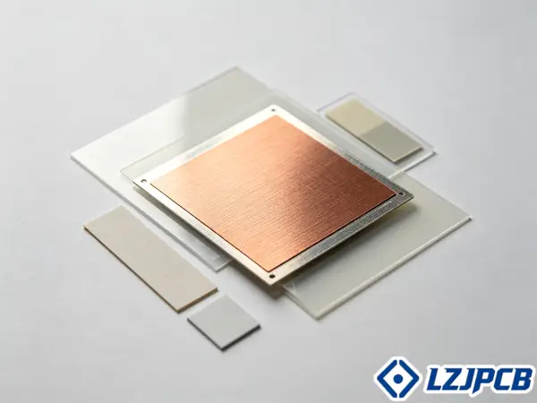
I have run over 300 PCB projects across 20+ countries. I have seen good designs fail because someone picked FR-4 for a 28 GHz antenna. Let me walk you through how I choose, so you never make that mistake.
How to Select the Right 5G PCB Material for Your Application
Pick the wrong material and your 5G board loses signal, heats up, and warps. The stakes are high. Selection starts with your frequency band.
To select the right 5G PCB material, first define your frequency band, then match the material’s Df, Dk, and cost to that band. Sub-6 GHz allows Df of 0.004 or less. mmWave needs lower Df and tighter control. Cost rises as loss drops.
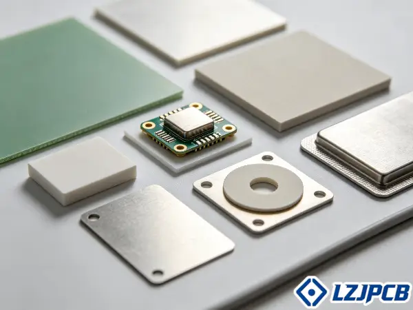
Standard FR-4 fails above 24 GHz. It shows signal loss, heat buildup, and dimensional drift. So for 5G, you almost always name a specific laminate in your files. You do not leave the choice to the fabricator. Let me break the decision into two parts.
Sub-6 GHz vs mmWave Band Selection
Your first job is knowing which band you serve. 5G splits into two groups. Sub-6 GHz runs below 6 GHz. mmWave runs at 24 GHz and above, centered near 26, 28, and 39 GHz. The band changes everything about material choice.
Sub-6 GHz is more forgiving. A material with Df of 0.004 or less works well here. Rogers RO4730G3, with a Dk near 3.0 and Df around 0.0028, fits sub-6 GHz antennas. Both Rogers and PTFE perform fine at these speeds. So I often pick Rogers. It costs less and processes easier.
mmWave is harsh. At 24 GHz and up, small losses stack fast. You need Df well below 0.004. Here I lean toward PTFE, with Df near 0.0009. The list below shows my quick band-to-material guide:
- Sub-6 GHz (below 6 GHz): Rogers RO4000 series or modified epoxy laminates
- Low mmWave (24–28 GHz): Rogers RO4000 or PTFE
- High mmWave (39 GHz and up): PTFE for lowest loss
Most early 5G builds sit in sub-6 GHz. But mmWave use keeps growing. So plan your material with the future in mind.
Cost vs Performance Trade-Off
Better electrical performance costs more money. This is the core trade-off. PTFE gives the lowest loss but sits at the top of the cost ladder. Hydrocarbon ceramics like Rogers sit in the middle. Modified epoxy systems cost the least among specialty options.
Choosing a specific brand and type brings three costs: higher price, minimum order quantities, and longer lead times. These hit every production run. So I qualify two or three materials that meet the same functional target. This gives you supply chain flexibility when one option runs short.
The table below shows the cost hierarchy I use with clients:
| Material Class | Relative Cost | Processing | Typical Use |
|---|---|---|---|
| PTFE laminates | Highest | Hard, needs special handling | mmWave, critical RF |
| Hydrocarbon ceramic (Rogers) | Medium | FR-4 compatible | RF front-end, antennas |
| Modified epoxy (Megtron, Isola) | Lowest specialty | Easy, mixes with FR-4 | High-speed digital, mixed boards |
For sub-6 GHz phone antennas in the n77 and n78 bands, cost analysis usually favors Rogers. You get the performance you need without paying the PTFE premium. Match the spend to the frequency, not to the marketing.
Key Electrical Parameters for 5G PCB Material
Two numbers decide if your board works: how much signal it loses and how stable its speed stays. Get these wrong and data corrupts.
The two key electrical parameters for 5G PCB material are dissipation factor (Df) and dielectric constant (Dk) stability. Df should be 0.004 or less for sub-6 GHz. Dk must stay steady across frequency and temperature to hold impedance and phase.
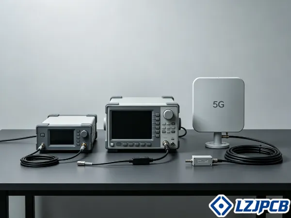
High-frequency materials must cut signal attenuation and dielectric loss. Attenuation weakens the signal. Dielectric loss turns energy into heat. Both hurt antennas, RF modules, and high-speed circuits. You also cannot copy a spec from 1 GHz to 24 GHz. So always use manufacturer data measured at your target frequency. Let me split these into the two properties that matter most.
Dissipation Factor Requirements
A low Df is non-negotiable for 5G. Df, also called loss tangent, sets how much signal dies as heat over your trace length. A lower Df means less wasted energy and cleaner data.
For sub-6 GHz, aim for Df of 0.004 or less. For mobile GHz work, I prefer below 0.005. For mmWave, go lower still. FR-4 sits at 0.02 to 0.03. That is one to two orders of magnitude worse than high-frequency laminates at 0.001 to 0.005. So FR-4 cannot serve a 5G front end.
Here is why the gap matters. A material with Df near 0.001, like PTFE at 0.0009, loses under 0.1% of energy per cycle at 10 GHz. A material at 0.005 loses 0.5%. That is a 5x difference. In high-power RF, that gap becomes real heat you must remove.
The list below shows my Df targets by application:
- Sub-6 GHz RF: Df of 0.004 or less
- Mobile GHz circuits: Df below 0.005 preferred
- mmWave (24 GHz+): Df below 0.002, PTFE range
- Power amplifiers: low Df plus high thermal conductivity
Remember: "low Df" is not one fixed number. It depends on your circuit type and band.
Dielectric Constant Stability
Dk stability is the primary electrical property for high-frequency work. Dk sets your signal speed. When Dk shifts, your impedance shifts too. That causes reflections, lost power, and higher bit error rates.
Makers specify Dk as a tolerance, like ±0.02, across a frequency range. That small tolerance can push impedance variation to around ±1 to 2% for a set trace shape. So a tighter Dk means tighter impedance control. Rogers materials, being ceramic-filled composites, hold a stable Dk across a wide range of conditions. Their Dk runs from about 2.2 to 10.2, giving you room to tune impedance and signal speed. PTFE is locked near 2.1.
Temperature matters as much as frequency. Antennas sit outdoors and face wide swings. So I check TCDk, the temperature coefficient of Dk. A TCDk near 50 ppm/°C is good. Closer to zero is better. Rogers RO4730G3 shows a TCDk around −26 ppm/°C. That gives strong frequency stability for antennas. Dk is common to all laminates, but TCDk is not uniform. You must check it per material.
Thermal and Mechanical Considerations for 5G PCB Materials
Fast signals make heat. Heat makes boards expand. Mismatched expansion cracks joints and lifts copper. So thermal design is not optional for 5G.
Thermal and mechanical selection for 5G PCB materials centers on thermal conductivity and CTE matching to copper. Aim for thermal conductivity of 0.50 W/m-K or higher. Match the material CTE close to copper’s ~17 ppm/°C to survive thermal cycling in outdoor base stations.
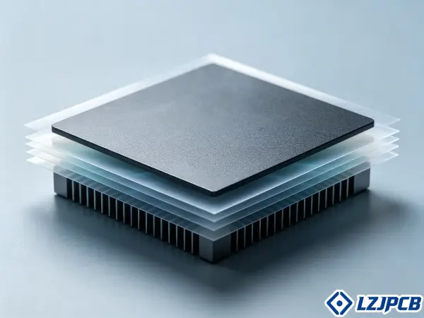
Heat scales with insertion loss. Circuits with higher loss dump more energy as heat. Too much heat lifts copper, delaminates layers, and warps the board. Higher speed also raises EMI. So material choice drives both how much heat you make and how well you move it away. Let me split this into the two key mechanical checks.
Thermal Conductivity Requirements
Thermal conductivity decides how fast a board moves heat to a heatsink. Higher conductivity means better cooling and less throttling in dense 5G parts. The benchmark for a "good" thermal conductor is 0.50 W/m-K.
Here is the hard part. Few low-loss laminates reach above 0.50 W/m-K. That creates a trade-off between low loss and good heat transfer. Rogers TC350 Plus breaks this pattern. It hits about 1.24 W/m-K, roughly 2.5x the benchmark, while keeping Df near 0.0017. So I reach for it in power amplifier circuits, which run hot and need both traits.
The list below shows where high thermal conductivity pays off:
- Power amplifier circuits: highest heat, needs TC350-class material
- Antenna feed structures: local hot spots near feed points
- Dense mmWave modules: little room for airflow
- Outdoor base stations: wide ambient range from −40°C to +55°C
You can also add thermal vias under power parts. Copper vias move heat from the pad to internal ground planes. In extreme cases, use metal-core boards or bonded heatsinks. Plan cooling from the start, not after the layout is locked.
Coefficient of Thermal Expansion Matching
CTE mismatch with copper is a top failure cause in high-power RF. When a board heats and cools, layers expand at different rates. That stress cracks plated holes and breaks connections. So you want the material CTE close to copper’s ~17 ppm/°C.
PTFE runs hot here. Its CTE sits around 70 to 150 ppm/°C, far from copper. That gap creates real risk in thermal cycling. Rogers ceramic-filled composites help. They land around 20 to 50 ppm/°C, much closer to copper. FR-4 in-plane CTE runs 14 to 17 ppm/°C, but its z-axis CTE jumps above Tg. So z-axis behavior matters most for hole reliability.
The table below compares CTE for common choices:
| Material | CTE (ppm/°C) | Match to Copper | Note |
|---|---|---|---|
| Copper | ~17 | reference | baseline |
| Rogers RO4000 (ceramic-filled) | 20–50 | good | reliable cycling |
| FR-4 (in-plane) | 14–17 | moderate | z-axis worse above Tg |
| PTFE | 70–150 | poor | needs care in cycling |
For outdoor 5G base stations, temperature swings are wide. So pick a material with closer CTE matching to survive years of cycling. This choice protects your via barrels and your solder joints.
5G PCB Materials Manufacturing
Great material means nothing if the factory cannot process it right. Soft PTFE smears. Vias leave stubs. One bad step kills signal integrity.
5G PCB materials manufacturing depends on lamination and drilling compatibility plus strict signal integrity testing. Rogers processes like FR-4. PTFE needs special handling. Every high-frequency trace must be tested as a controlled impedance line, usually 50Ω.
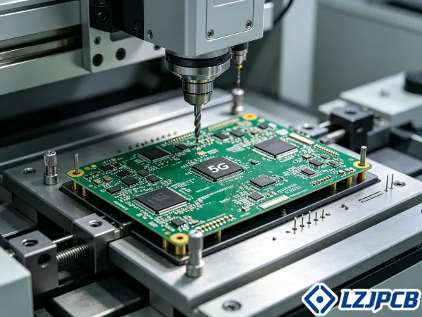
At LZJPCB, our Ji’an city base runs 1 to 40-layer boards with impedance control at ±5%. We use back drilling, blind and buried vias, and HDI to handle high-frequency needs. I bring our engineers into your design early. This is where most competitors fall short. They rely on web ordering. We give you one-on-one support so the board works. Let me show the two steps that decide success.
Lamination and Drilling Compatibility
Not every material runs on the same line. Rogers RO4000 series is compatible with FR-4 processing. So we build these boards on existing equipment without big retooling. That saves cost and time for you.
PTFE is harder. It is soft, so it smears and burrs during drilling and routing. It needs special drill and route parameters. Its lower dimensional stability also means we plate with high-tensile-strength copper to stop cracks and bending. So PTFE yields tend to run lower than Rogers in high-volume runs. That is a real production factor, not just a spec sheet note.
Here is my process checklist for high-frequency builds:
- Confirm the laminate is named in the fabrication files
- Match press cycle and temperature to the material class
- Set drill parameters for soft PTFE to avoid smear
- Use low-profile copper foil to cut conductor loss
- For hybrid boards, use proper bondply between PTFE and FR-4 layers
- Manage differential expansion in mixed material stack-ups
Hybrid designs mix Rogers or PTFE RF layers with FR-4 digital layers. This balances cost, performance, and manufacturability. But the bonding interface needs care to prevent delamination. So we treat and inspect it as an extra step.
Signal Integrity Test Methods
Signal integrity at high frequency is almost all about impedance control. Any deviation creates reflections. Those reflections get worse as frequency climbs. So we design every RF trace as a controlled impedance line, microstrip or stripline, and target 50Ω.
Copper surface roughness matters here too. Smoother, low-profile copper cuts insertion loss. The skin effect pushes current near the surface, and the effect grows with the square root of frequency. So above 10 GHz, HVLP copper makes a clear difference. We also back-drill vias to remove stubs that resonate and degrade the signal at GHz speeds.
The list below shows my core test and design steps:
- 100% electrical test plus AOI dual inspection on every board
- Controlled impedance test to verify 50Ω target
- Apply the 3W rule to reduce crosstalk between traces
- Keep a signal layer next to a reference plane for return paths
- Use via fencing near RF sections to contain fields
- Simulate transitions, filters, and antennas with a 3D field solver first
We keep high-frequency paths short and direct. We avoid sharp angles and use arcs instead. And we validate material models by simulation before we cut copper. This cuts costly design loops and gets your board right the first time.
FAQ About 5G PCB Materials
These FAQs cover the most common 5G PCB material questions on FR-4 limits, PTFE versus Rogers, and thickness rules. Short answers first, so you can decide fast.
Why can’t I use standard FR-4 for 5G?
FR-4 fails above 24 GHz. It shows three problems: signal loss, heat buildup, and dimensional drift. Its Df of 0.02 to 0.03 is far too high for RF front ends. So it works below about 5 Gbps only.
Should I choose PTFE or Rogers?
It depends on your goal. PTFE gives the lowest loss at Df near 0.0009 and suits demanding mmWave. Rogers offers a wide Dk range of 2.2 to 10.2, easier processing, and lower cost. For most sub-6 GHz work, I pick Rogers.
How thin should my board be?
Thinner boards cut signal travel distance and lower attenuation. But they must stay strong for compact devices. Laminate thickness is often set as a fraction of the operating wavelength, like 1/8 to 1/4, to avoid resonance.
What Df do I need for mmWave?
Below 0.004 is a starting point. For mmWave, go lower, toward the PTFE range near 0.001. Every fraction of a dB adds up over your antenna feed network at 28 GHz.
Do you support material selection?
Yes. Our supply chain team and engineers help you qualify two or three material options. We source from Rogers, Isola, Panasonic, Shengyi, and more, all genuine and traceable. So you get performance and supply flexibility.
Conclusion
Choose 5G PCB materials by band, Df, Dk stability, thermal conductivity, and CTE. PTFE and Rogers lead. Match material to frequency, and partner early with your fabricator.