Skip to content
The top 10 high frequency PCB manufacturers combine specialty materials, tight impedance control, and fast delivery to handle boards above 500MHz. Below is my ranked list based on materials, certifications, and technical support.
- LZJPCB — Best for turnkey custom RF work with 1-on-1 engineer support, Rogers and PTFE materials, 5 day prototypes.
Found: 2006
Employees: 500+
Email: Jayden@Lzjpcb.com
WhatsApp: (86) 133-1654-3659
factory: 3 in China and 1 in Indonesia
Certifications: ISO 13485, IATF 16949, ISO 9001, ISO 1400, REACH, RoHS
Address: Building B2, Tantou 3rd Industrial Zone, Songgang Street, Bao’an District, Shenzhen, China
- Rogers-certified fabs — Strong for premium RO4350B and RT5880 laminates above 10GHz.
Email: solutions@rogerscorp.com
Address: 2225 W. Chandler Blvd., Chandler, AZ 85224
- Isola-based makers — Good mid-tier for 5-25 Gbps designs at lower cost.
Tel: 800-537-7656
Email: amer.customer.service@isola-group.com
Address: 6565 West Frye Chandler, AZ 85226
- Taconic specialists — Solid PTFE options like RF-35 and TLY-5 for microwave bands.
Email: info@4taconic.com
Address: 136 Coonbrook Road, Petersburgh, NY 12138, USA
- Nelco fabs — Reliable for high-speed digital between FR4 and Rogers.
Tel: +1 (631) 465-3600
Email: sales@nelcoproducts.com
Email: info@nelcoproducts.com
Address: 1400 Old Country Road, Suite 409N, Westbury, NY 11590, USA
- Panasonic Megtron — Best for high-speed backplanes and servers.
Tel: +886-3-598-3201
Email: pidmtw-qa@tw.panasonic.com
Address: V2CF+2P Zhongxing Village, Hukou Township, Hsinchu County, Taiwan
- PTFE Teflon experts — For ultra-low-loss work above 20GHz.
Tel: (909) 987-9533
Email: contactus.ranch@arlonemd.com
Address: 9433 Hyssop Drive, Rancho Cucamonga, CA 91730, United States
- TTM Technologies — Hybrid stackup fabs Balance cost and performance with sandwich builds.
Tel: (408)486-3100
Address: 200 East Sandpointe, Suite 400, Santa Ana, CA 92707, USA
- Sanmina — Quick-turn prototype houses, Fast 24-72 hour turnaround, limited materials.
Tel: +1 408 964-6400
Email: info@sanmina.com
Address: 2050 Bering Drive San Jose, CA 95131 United States
- AT&S — advanced HDI and rigid-flex circuits supporting frequencies over 100 GHz.
Tel: +43 3842 200-0
Email: privacy@ats.net
Address: Fabriksgasse 13, 8700 Leoben, Austria

Picking from this list is only the start. You need to know what makes a real high frequency PCB manufacturer stand out. Let me break it down.
What Is a High Frequency PCB Manufacturer?
Many buyers confuse standard PCB shops with true RF fabs. This mistake leads to bad signals and wasted boards. The difference is real and important.
A high frequency PCB manufacturer builds boards that carry signals above 500MHz, often into the GHz range, using special materials and tight process controls. Standard FR4 loses too much signal past this point. These fabs manage dielectric constant, loss, and impedance with precision.
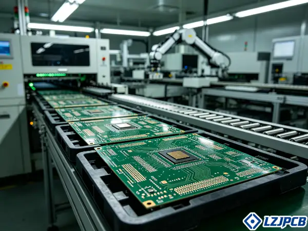
I have worked on more than 300 PCB projects across 20 countries. High frequency work sits in its own class. When a circuit runs above 500MHz, signal losses in normal FR4 rise fast. The industry uses a few frameworks to define "high frequency." One common threshold is 50MHz, where electromagnetic radiation starts to affect nearby circuits. Another view splits devices by band: low frequency below 25MHz, medium 25-100MHz, high 100-1000MHz, and ultra-high above 1000MHz. A third view looks at signal travel time. When signal travel time passes 1/3 of the switching time, transmission line effects take over. At 500MHz, the wavelength is about 60cm. Board size then matters electrically. This is why a real high frequency fab treats signal physics as the core job, not just connecting parts.
PCB Materials for High Frequency Boards
The material is the heart of a high frequency board. Standard FR4 hits a wall as frequency climbs. That wall is why specialty laminates exist. Three electrical parameters set these materials apart from normal boards: dielectric constant (Dk), dissipation factor (Df), and coefficient of thermal expansion (CTE).
High frequency PCB materials must do three things at once. They need good electrical performance, low dielectric loss, and stable behavior under heat and humidity. The numbers show the range. Dk runs from 2.2 to 10.2. Df runs from 0.0009 to 0.004. Thickness runs from 0.2mm to 8.0mm. That is a wide spread across available laminates.
Here are common materials I use and their key values:
| Material | Dk (at 10GHz) | Df | Notes |
|---|---|---|---|
| Rogers RO4350B | 3.48 | 0.0037 | Cost-performance sweet spot, sub-6GHz 5G |
| Rogers RO4003C | 3.38 | Low | General-purpose RF |
| Rogers RO3003 | 3.00 | Low | Microwave use |
| Rogers RO3010 | 10.2 | Low | High Dk designs |
| Rogers RT5880 | 2.20 | ~0.0009 | Lowest Dk, tightest tolerance |
| PTFE ZYF255DA | 2.55 | 0.0018 | Ultra-low loss |
| PTFE ZYF300CA-P | 3.0 | 0.0018 | Microwave bands |
FR4 still works for clock rates below 5 Gbps at much lower cost. Rogers and PTFE take over above 10GHz where loss budgets tighten. We also offer hybrid sandwich builds. High frequency laminates go on outer layers. Inner layers use standard epoxy glass cloth. This cuts cost while keeping performance where it counts.
Impedance Control and Signal Integrity
Impedance control keeps your signals clean. Poor control causes reflections that ruin performance. This is where many cheap fabs fail.
Controlled impedance matches the transmission line impedance to source and load. This minimizes signal reflections. We hold tolerance at ±10%. At a 50Ω target, this allows a 45-55Ω range. That is tighter than standard PCB tolerance of ±15% but looser than aerospace-grade ±5%. The standard values in RF work are 50Ω, 75Ω, and 100Ω.
Impedance comes from matching trace width and spacing to the stack-up and material Dk. This makes pre-production simulation a must. Lower Dk lets us use wider traces for the same 50Ω target. Wider traces reduce conductor loss and improve manufacturing.
Signal integrity also depends on the transmission line type. There are two main choices:
- Microstrip — On outer layers with one reference plane. Easier to access and debug.
- Stripline — On inner layers with two reference planes. Better shielding but harder vias.
Above 10GHz, copper foil type matters a lot. Rough copper surfaces raise conductor loss by 35% due to the skin effect. AC current crowds near the surface at high frequency. We use low-profile copper to fight this. We verify final results with TDR (Time Domain Reflectometry) testing. This shows impedance changes along each trace and finds discontinuities before they cause failures in the field.
How to Evaluate High-Frequency PCB Suppliers?
Buyers often pick on price alone. This backfires with bad quality and slow shipping. A structured check protects you.
Evaluate high frequency PCB suppliers on material range, impedance capability, certifications, lead time, and technical support. Score technical capability at 40%, quality record at 30%, cost at 20%, and lead time at 10%. This gives you an objective, fair choice.
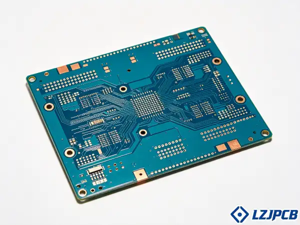
One of my buyer colleagues in the United States always examines the industry experience of the suppliers first. That is the right instinct. Ask if the fab has built boards for your field. Ask about hidden costs too. Beyond the quoted unit price, you often see NRE fees ($500-$5,000), stencil charges ($100-$400), test fixtures ($500-$5,000), and shipping. These can add 15-40% to total project cost. Also check supply chain resilience. Fabs with dual sourcing and buffer stock reduce your disruption risk. This matters more since the 2020 semiconductor shortages.
Production Lead Times for High Frequency PCBs
Lead time affects your whole product schedule. Long waits break your market plans. This is a real pain point for buyers who serve many markets.
Production lead time for high frequency PCBs ranges from 2 days expedited to 5 weeks for complex orders. This 17.5x range links directly to layer count, material stock, and process complexity. At LZJPCB, a 2-layer high frequency board ships in 4-5 days for prototyping. That is faster than the 7-10 day industry average for Rogers or PTFE prototypes.
Here is a typical lead time breakdown:
- Prototype — 24-72 hours for most designs.
- Expedited — 2-3 days.
- Regular production — 7-10 days.
- Complex multilayer — Up to 5 weeks.
Standard lead time has three parts. Engineering and CAM prep take 8-24 hours for complex designs. Fabrication takes 3-5 days for standard boards. Assembly takes 2-4 days based on part count. A short lead time often means a streamlined process with fixed stackups and limited material options. Ask what tradeoff sits behind a fast quote. Sometimes speed means less flexibility. My team runs 7×24 service so we keep progress moving on urgent RF orders, which helps you track and plan.
Quality Certifications for High Frequency PCB Manufacturing
Certifications prove a fab meets real standards. Without them, you gamble on quality. For regulated fields, this is not optional.
Quality certifications for high frequency PCB manufacturing should include ISO 9001, IATF 16949 for automotive, and IPC-A-610 Class 2/3 acceptance. We hold ISO9001, ISO14001, IATF16949, ISO13485, UL, CUL, RoHS, and REACH. We also have 20+ patents and China National High-Tech Enterprise status.
IPC class matters for reliability. Here is the difference:
| IPC Class | Use Case | Reliability |
|---|---|---|
| Class 2 | Commercial, industrial | Standard, dedicated service |
| Class 3 | Aerospace, defense | Highest, performance-on-demand |
We offer both Class 2 and Class 3 compliance. Class 3 is for products where continued performance is critical. RoHS compliance is mandatory for EU and most global markets. REACH, UL 94 V-0 flammability, and ITAR for defense each add process and documentation needs. These raise cost based on audit frequency. We run 100% electrical testing and AOI inspection on all boards. We also provide free DFM and DFT checks. Functional testing is available on request. A comprehensive supplier check should confirm these match your industry. This is precisely the key point that PCB buyers focus on when purchasing from China.
What Affects High Frequency PCB Costs?
Price surprises frustrate every purchaser. You think you know the cost, then extras appear. Understanding cost drivers saves your budget.
High frequency PCB costs depend on material grade, layer count, setup fees, surface finish, and impedance verification. Material is often the biggest driver. A 2-layer high frequency board can start at $47 for 5 pieces. Premium PTFE and tight tolerances push this higher.
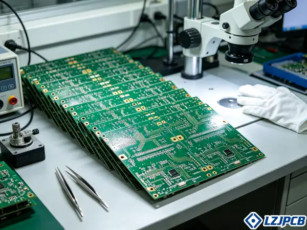
Cost is never just the unit price. Panel utilization matters too. A 5% gain in panel use cuts per-board material cost by 5%. Fabs with in-house panel optimization hold a 5-15% cost edge. Surface finish adds cost as well. HASL costs less than ENIG but gives shorter shelf life and poorer flatness for fine-pitch parts below 0.5mm. Component sourcing changes cost too. Turnkey assembly adds 8-15% markup but cuts your procurement work. I always show buyers where each dollar goes, so there are no hidden surprises later.
Material Grade vs Cost Tradeoffs
Material choice drives both price and performance. Pick too high a grade and you overpay. Pick too low and signals fail. The balance is key.
Material grade vs cost follows a threshold model. FR4 works below 5 Gbps at low cost. Nelco, Isola, and Megtron fit the 5-25 Gbps band as mid-tier. Rogers and RT/duroid handle above 56 Gbps but cost more due to special processing.
Here is how the tiers stack up:
| Material Tier | Clock Rate | Cost | Best Use |
|---|---|---|---|
| FR4 | Below 5 Gbps | Lowest | Simple RF, budget designs |
| Nelco/Isola/Megtron | 5-25 Gbps | Mid | High-speed digital |
| Rogers hydrocarbon | Sub-6GHz to 56 Gbps | Premium | 5G, microwave |
| PTFE Teflon | Above 20GHz | Highest | Ultra-low-loss RF |
Rogers RO4350B sits at the cost-performance sweet spot. It suits most sub-6GHz 5G work. PTFE materials give lower Df but cost more and are harder to make. PTFE has dimensional instability, drill smear, and plating adhesion issues. It needs plasma treatment or sodium etching. This is why PTFE stays a premium upgrade. My advice: match material to your real frequency need. Use hybrid sandwich builds when you can. Put premium material only on layers that need it. This is the smartest way to control cost without hurting signal quality.
Setup Fees for High Frequency PCB
Setup fees catch many first-time buyers off guard. These one-time costs hit small orders hard. Knowing them upfront helps you plan.
Setup fees for high frequency PCB include NRE, stencil, and test fixture charges. NRE fees run $500-$5,000 per project. Stencil charges run $100-$400 per stencil. Test fixtures run $500-$5,000. These are one-time costs that spread across your order volume.
For low volume, testing choice affects setup cost:
- Flying probe testing — No fixture cost. Adds 2-5 minutes per board. Best for 1-50 units.
- Bed-of-nails fixture — Fixture costs $500-$5,000. Drops below $1/board above 1,000 units.
For prototype runs of 1-50 units, flying probe is more economical. It removes the fixture cost. For volume, the fixture pays off. Engineering change orders also cost more during production than in prototyping. This is why I push for design freeze before volume. Catch changes early and you avoid costly retooling. We support orders from 1 piece to 10,000+ pieces. This lets you prototype cheaply, then scale without switching fabs. Keeping one partner across the full cycle reduces your setup cost over time.
High Frequency PCB Prototype
Prototypes make or break your development timeline. A slow or wrong prototype delays your whole product. Fast, accurate prototypes keep you moving.
High frequency PCB prototypes should ship in 24-72 hours with DFM feedback before production. We build 2-layer high frequency prototypes in 5 days starting at $50 for 5 pieces. Most designs need 4 iterations before design freeze.
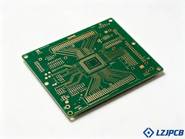
Prototyping usually needs 5-10 units per iteration. The NPI phase averages 4 design cycles before freeze. Each cycle costs 10-20% of final unit pricing when spread over total NRE. My team runs parallel design work 7×24. This cuts iteration time. We give engineering feedback fast during quoting and review. This lowers your re-spin count. The goal is simple: get your RF board right in fewer tries, so you launch on schedule.
Quick-Turn Prototype Services
Quick-turn service saves days when your schedule is tight. Waiting a week for a prototype can miss a market window. Speed here matters.
Quick-turn prototype services deliver high-frequency boards in 24-72 hours for most designs. Expedited orders ship in 3 days. The ordering process requires uploading Gerber files for production.
To use quick-turn well, follow these steps:
- Prepare Gerber files — You need a complete layout from RF-aware routing tools.
- Confirm material — Fast turns often use fixed stackups and limited materials.
- Set quantity — Start from 1 piece for research, scale to 10,000+ for production.
- Choose finish — ENIG is standard for RF due to flatness.
- Submit for DFM — Free checks catch issues before build.
5-day turn is short against the 7-10 day average for Rogers or PTFE. This speed comes from a streamlined process. Note that fast service may not offer design help. You must have your layout ready. We do not generate files for you at this tier. This is fine for buyers who design in-house, like most of my clients. They bring a finished RF layout and just need fast, accurate fabrication.
Design for Manufacturing Feedback
DFM feedback prevents problems before they cost you money. A board that looks fine in CAD can fail in the fab. Early feedback fixes this.
Design for manufacturing feedback flags issues in your layout before production starts. We provide free DFM and DFT checks. This lets you validate your design before you commit to a build. Fabs that give DFM feedback lower first-pass failure rates.
I always recommend early collaboration. Work with us during planning to verify stack-up, impedance calculations, and layout rules. This step prevents costly re-spins. Material and impedance choices must come first. Dk and Df values set the etch compensation, drilling parameters, and plating chemistry. The planning phase should also document your maximum frequency, fastest switching rate, and power needs. We check minimum tolerance requirements against our capability. A checklist-based plan prevents delays and surprises. High frequency design has many variables at once: impedance, timing, EMI, and thermal. Systematic pre-work handles them. My team joins your planning to align electrical needs with what the fab can actually build. This is where 1-on-1 engineer support pays off most.
Technical Support for High Frequency PCBs
Weak support leaves you stuck when problems appear. Most fabs just take your files and build. Real support guides you through the hard parts.
Technical support for high-frequency PCBs covers stackup design, signal integrity simulation, and after-sales help. We assign dedicated engineers to each project. This is different from website-based order platforms that offer no customization.
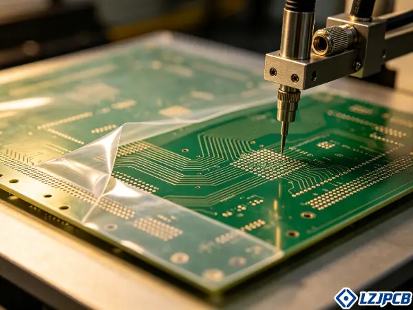
Our team has 50+ engineers, with 30+ holding 5-12 years of experience. We support up to 28 layers, 112G signal speed, and 2.5mil trace/space. This depth lets us solve real RF problems, not just fabricate. Support factors also include RMA policies, warranty periods, and failure analysis. Standard warranty covers 12 months for manufacturing defects. These affect your total cost of ownership. I have seen many projects saved by good support at the right moment.
Stackup Design Assistance
Stackup design sets the foundation for your RF board. A bad stackup ruins impedance and adds EMI. Getting it right early saves everything downstream.
Stackup design assistance helps you plan layer order, materials, and impedance. Every signal layer should sit next to a plane layer for a low-impedance return path. High-speed signals belong on inner layers between planes for shielding.
Key stackup rules I apply:
- Solid ground plane — Place a continuous, unbroken ground under high-speed traces.
- Adjacent planes — Every signal layer needs a power or ground plane next to it.
- Multiple grounds — Extra ground layers lower impedance and cut common-mode emissions.
- 20H rule — Recess the power layer by 20 times the dielectric thickness from ground. This absorbs edge flux and cuts EMI radiation.
- Ground bridges — If a ground break is unavoidable, add a 0-ohm resistor to bridge the return path.
We support layer counts from 2 to 24 layers. Prepreg choice affects the whole stackup Dk. We offer Rogers 4450F and domestic options like 25FR, RF-27, and 6700 for cost control. A 2-layer service limits complex designs. Buried stripline or plane isolation needs 4 or more layers. I help each client pick the layer count that fits both their signal needs and their budget. This early work prevents the impedance surprises that plague rushed designs.
Signal Integrity Simulation Support
Simulation catches signal problems before you build. Physical prototyping to find issues is slow and costly. Simulation is faster and cheaper.
Signal integrity simulation support lets you validate electrical performance before physical prototyping. We provide impedance simulation for stack-up and trace design. This confirms your board will perform before you spend on prototypes.
Four invisible forces hurt high-frequency performance: mutual interference, electromagnetic interference, signal reflections, and crosstalk. Each needs its own fix. We apply key layout rules:
- 3W rule — Keep trace centerlines at least three trace widths apart to cut crosstalk.
- Avoid 90° corners — Use 45° angles or curves to stop reflections.
- Orthogonal routing — Route adjacent layers at right angles to cut broadside coupling.
- Match differential pairs — Keep equal lengths and constant spacing for common-mode rejection.
- Minimize vias — Each via adds impedance discontinuity and parasitic inductance.
Isolate analog, digital, and power into three zones. This cuts interference between blocks. Higher baud rates make signal integrity harder, with EMI as the main cause of degradation. At 25 Gbps today, challenges are far worse than the 3 Gbps norm of 2005. Simulation guides trace width, spacing, and via choices before build. My engineers run these checks so your first prototype comes back closer to right.
After-Sales Support
After-sales support protects you when field problems appear. A board can pass tests then fail in use. Good support handles that.
After-sales support includes RMA policies, warranty coverage, and failure analysis. Our standard warranty covers 12 months for manufacturing defects. We also provide engineering support for field failures. These factors shape your total cost of ownership.
Many companies worry about PCB after-sales help, and that concern is valid. When a board fails in the field, you need answers fast. We offer multi-point technical support and 7×24 online service. Our engineers can run failure analysis to find the root cause. This matters most in medical, AI-robot, and industrial work where failures are costly. Test coverage during production reduces field failures first. Visual inspection catches 50% of visible defects. AOI catches 80% of soldering defects. X-ray catches 95%+ of hidden BGA issues. ICT catches 85-98% of electrical faults. A defect rate below 100 ppm marks high-quality assembly. We back all of this with a real support team, not just an order page. This is the win-win partnership I aim for with every client, from prototype through years of production.
FAQ About High Frequency PCB Manufacturers
What frequency counts as high frequency?
High frequency PCB work becomes necessary above 500MHz, where signal losses in standard FR4 rise sharply. Many designs extend into the GHz range. The EMI threshold is often set at 50MHz.
Can I use FR4 for high frequency boards?
Yes, for clock rates below 5 Gbps. FR4 gives enough impedance control at much lower cost. Above 10GHz, you need Rogers or PTFE materials for tighter loss budgets.
What is the best material for RF PCBs?
Rogers RO4350B offers the best cost-performance balance for sub-6GHz 5G, with Dk of 3.48 and Df of 0.0037. PTFE materials serve frequencies above 20GHz.
What impedance tolerance should I expect? We hold ±10% for high-frequency boards. This gives a 45-55Ω range at a 50Ω target. It is tighter than the ±15% standard but looser than aerospace ±5%.
How fast can I get a prototype?
Most high-frequency prototypes ship in 24-72 hours. Our 2-layer boards ship in 4-5 days starting at $47 for 5 pieces.
Which surface finish is best for RF?
ENIG is most common for RF due to its flatness and oxidation resistance. Note that ENIG adds a nickel layer that can raise insertion loss at very high frequencies.
Conclusion
The best high frequency PCB manufacturers combine specialty materials, ±10% impedance control, fast prototypes, and real engineer support to solve your RF challenges.