Skip to content
Your high-frequency board fails EMC testing. Signals ring, timing slips, and the whole project stalls. One wrong material or one split ground plane can ruin months of work.
High-frequency PCB design means controlling electromagnetic energy on boards that run at 100 MHz and above, reaching into the gigahertz range. You do this by choosing low-loss materials, holding impedance tight, keeping a continuous ground return path, and separating analog from digital signals. These four steps protect signal integrity and cut EMI.
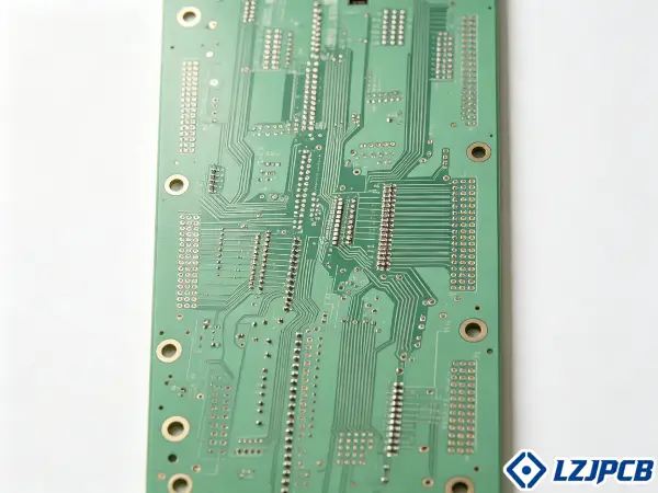
I have run more than 300 PCB projects over 7 years. I have seen what breaks at high frequency and what saves a design. Let me walk you through the rules that actually matter, step by step.
What Is a High Frequency PCB?
Many engineers confuse "high frequency" with "high speed." The mix-up leads to wrong material picks and failed boards. Let me clear it up.
A high frequency PCB is a board that operates at 100 MHz and above, extending into the gigahertz range. At these frequencies, signal integrity failures like ringing, crosstalk, reflections, and impedance mismatch appear. These effects change both digital timing and analog voltage levels.
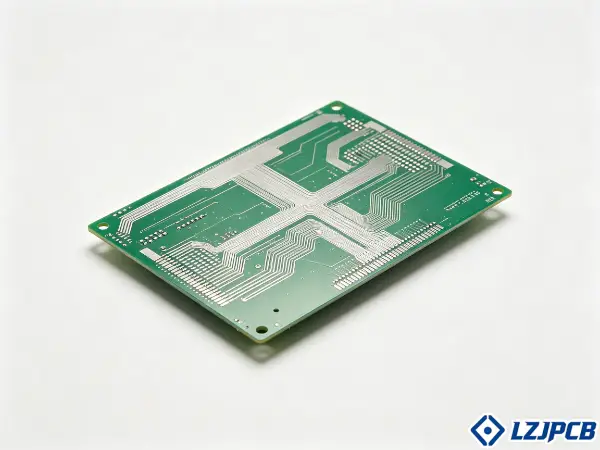
The reason this matters is simple. Below 100 MHz, standard IPC rules work fine. Above it, the physics change. Traces stop acting like simple wires and start acting like transmission lines. Now let me break down the two ideas engineers keep mixing up.
High Frequency vs High Speed PCBs
High frequency and high speed are not the same thing, but they overlap. I define them by different signal traits.
- High frequency is defined by frequency-domain traits. It refers to boards where analog or RF signals have a high cycle frequency, measured in Hz.
- High speed is defined by time-domain traits. It refers to boards that transmit or process digital signals at high data rates, measured in bits per second.
The functional impact is the same. In both cases, signal changes happen fast enough that impedance and board parameters hurt signal integrity. A board can be both at once. A microwave digital transceiver, for example, must handle RF and digital signal integrity together.
Here is the key point for classification. The fastest signal on the board sets the speed domain. This is based on the ratio of transition time to path travel time.
| Domain | Rule | Design Action |
|---|---|---|
| Slow | Transition time within ¼ of travel time | Standard IPC rules are enough |
| Fast | Frequency effects appear | Shorten signal paths to fix |
| High speed / high frequency | Effects dominate | Full high-frequency interventions needed |
For digital signals, classification depends on rise and fall times, not just bit rate. A signal with a moderate bit rate but very fast edges still shows high-speed effects. Fast edges carry high-frequency harmonics.
Frequency Thresholds for High Frequency Rules
The 100 MHz threshold ties to wavelength. When a trace length becomes a large fraction of the signal wavelength, transmission line effects take over.
At 100 MHz, the wavelength is about 3 meters in free space and roughly 1.5 meters on FR4. A common boundary is the λ/10 rule. Traces longer than about λ/10 usually need transmission line treatment. Some engineers use λ/20 for a stricter margin.
For RF signals, real impact starts around 50 MHz. A 50 MHz signal has a wavelength near 1.5 meters in FR4. So trace lengths past about 37.5 cm (λ/4) enter the high frequency regime.
- Propagation speed on a PCB trace is about c divided by the square root of the effective dielectric constant.
- This means a 1 ns rise time maps to roughly 15 cm of trace in FR4.
- That number sets the physical scale of "long" and "short" traces.
Critical design rules change fundamentally above 1 GHz. The margin for error shrinks. You need tighter tolerances on every parameter. These thresholds are rules of thumb. The exact point depends on your board geometry, dielectric, and trace lengths.
Common Signal Issues in High-Frequency PCBs
You designed the board right, but signals still corrupt. The cause is almost always reflection or crosstalk. These two problems ruin more high frequency boards than anything else.
The two most common signal issues in high-frequency PCBs are signal reflection from impedance discontinuity and crosstalk between adjacent traces. Both come from the same root: at high frequency, energy couples and bounces in ways it never would at low frequency. Noise and EMI then disrupt data fidelity.
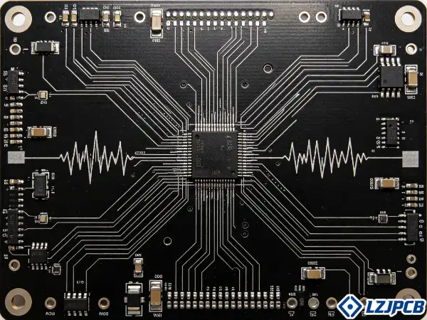
There are more issues, such as harmonic distortion, common-mode noise, and surface tracking. But reflection and crosstalk hit first and hit hardest. Let me show you why.
Signal Reflection From Impedance Discontinuity
Signal reflection happens when a signal hits a point where impedance changes. Part of the energy bounces back toward the source instead of moving forward.
Any discontinuity causes this. A via, a connector pad, or a sharp trace angle all act as reflection points. The bounced energy corrupts the signal. You see it as ringing, overshoot, and undershoot on the waveform.
The fix is impedance matching. Every high-frequency trace must be treated as a transmission line, not a plain conductor. You match the source and load impedance across the whole path.
- Signal radiation intensity scales with routing length. Longer traces radiate more and couple more.
- Mismatched differential pairs add reflection. So does excess trace length and missing shielding.
- Connector pads create discontinuities at every connection. Design the pad as part of the transmission line.
Harmonic distortion is a related problem. It produces frequency shifts that degrade signals and hurt transmit and receive systems. You can add low-pass or band-pass filtering at the output to cut it, but that adds insertion loss. This is a trade-off you must weigh for each design.
Crosstalk Between Adjacent Traces
Crosstalk is unwanted coupling between two nearby traces. Energy from one trace jumps to another and corrupts it.
Four independent variables set crosstalk magnitude:
- PCB layer stack parameters
- Signal line spacing
- Electrical characteristics of source and load terminals
- Signal line connection mode
This means layer stack-up is a critical input, not a small detail. The physical parameters of the layers decide how much energy couples. Coupling is also frequency-dependent. Higher frequency raises coupling for the same spacing, so you need wider spacing at higher frequency.
The main defense is the 3W rule. Keep the center-to-center distance between two traces at least three times the trace width. You can also use the 3H version, spacing traces at least three times the dielectric height from the reference plane.
Other methods help too:
- Route clock lines perpendicular to other lines to cut parallel coupling length.
- Insert a ground plane between signal lines as a shielding barrier.
- Surround clock lines with ground lines plus stitching vias for isolation.
- Minimize parallel run length between adjacent signals.
Parasitic capacitance is a big source of coupling. You cannot fully remove it, but you can minimize it. Increase conductor spacing, pick a dielectric with lower permittivity, and shorten parallel trace lengths.
Material Selection for High Frequency PCBs
Pick the wrong laminate and no layout trick can save your board. Material selection is the first non-negotiable decision in high-frequency design.
For high-frequency PCBs, standard FR4 is too lossy, so you must select low-loss laminates such as Rogers RO4350B, Isola Astra, or Panasonic Megtron 6. These offer a stable dielectric constant and low dissipation factor across the operating frequency range. Above 1 GHz, the dielectric stops being a passive insulator and starts shaping signal behavior.
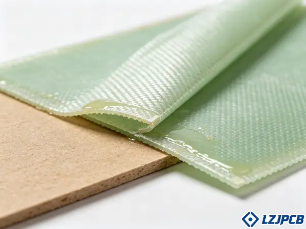
Material cost often dominates the total board cost, because high-frequency laminates can cost several times more than FR4. So this choice is also a major cost driver. Let me break down why FR4 fails and what the numbers should be.
Why FR4 Fails Above Certain Frequencies
FR4 fails at high frequency for two reasons. It is lossy, and its dielectric constant shifts with frequency.
Standard FR4 has a Dk that ranges roughly between 4.0 and 4.6. That is a range, not a single value. So impedance on an FR4 board can vary across the same panel with no routing change. The Dk can shift 5 to 10 percent from 1 MHz to 1 GHz. This causes unpredictable impedance and timing.
FR4 also has a high dissipation factor, roughly 0.015 to 0.025. This causes real signal loss and integrity failures above a few GHz. A square wave leaves the transmitter and arrives rounded and attenuated at the receiver.
- FR4 becomes problematic above a few GHz from both Dk drift and high Df.
- Any design in that range needs a material swap.
- The exact frequency where FR4 becomes fully unusable depends on your trace lengths and signal integrity budget.
I have seen teams try to push FR4 into 5 GHz designs to save money. The boards failed impedance testing every time. The lesson stuck.
Dk Requirements for Low-Loss Laminates
Dielectric constant (Dk) sets signal propagation speed. Higher Dk means slower signal velocity. So a stable Dk is the first material requirement.
Inconsistent Dk causes timing skew. This disrupts parallel buses and differential pairs. Dk dispersion, where Dk changes with frequency, makes different frequency parts of one signal travel at different speeds. That distorts the waveform.
| Material | Approximate Dk | Notes |
|---|---|---|
| Standard FR4 | 4.0 – 4.6 | Varies with frequency, unstable |
| Rogers RO4350B | ~3.48 (process Dk ~3.66) | Tight tolerance ±0.05 |
High frequency laminates like Rogers, Isola, and Taconic hold a tightly controlled Dk across both board area and frequency. You must characterize the material across your full operating bandwidth, not just at one spot frequency. The manufacturing consistency of the laminate decides whether your board performs the same across every production batch.
Df Requirements for Low-Loss Materials
Dissipation factor (Df), also called loss tangent, measures how much signal energy the dielectric absorbs and turns into heat. Lower Df means less loss.
Here are typical values at 10 GHz:
- High frequency materials: about 0.001 to 0.005 (Rogers RO4350B is around 0.0037)
- FR4: roughly 0.015 to 0.025
So specialty materials show several times lower dielectric loss than FR4. That directly cuts insertion loss and heat.
You reduce dielectric loss mainly by picking a low-Df laminate. But do not forget the solder mask. Solder mask has its own dissipation factor, and CMs often do not control its thickness tightly. For very high frequency designs above 5 GHz, you may need to remove solder mask from critical traces to cut variability.
Both Dk and Df change with temperature in most materials. So thermal management and your operating temperature range matter during selection. Material choice is a trade-off among Dk stability, Df, cost, and manufacturability. No single material wins on all four.
Controlled Impedance Design Rules
Signals reflect, ring, and overshoot. The root cause is nearly always uncontrolled impedance. Get this right and half your signal integrity problems disappear.
Controlled impedance design means keeping characteristic impedance constant from source to load, typically 50Ω for single-ended and 100Ω for differential signals. You do this with tight trace width control and proper stack-up. This prevents reflections. It is a foundational first step, not an optional add-on.
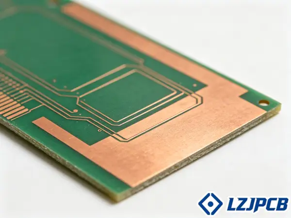
Impedance depends on three variables: trace width, height above the reference plane, and the Dk of the dielectric. Change any one and impedance shifts. Let me show you how to set and match it.
Setting Trace Width for a Target Impedance
Trace width is the main knob you turn to hit a target impedance. But it does not work alone.
You calculate trace width from three inputs:
- Copper thickness
- Dielectric height above the reference plane
- Dielectric constant (Dk)
The same trace geometry on a different material gives a different impedance. So material choice and trace geometry are coupled. You cannot set them separately.
You have two main transmission line structures to choose from:
| Structure | Description | Best For |
|---|---|---|
| Microstrip | Trace on outer layer, one reference plane | Shorter, non-critical paths |
| Stripline | Trace between two ground planes | Highly sensitive signals |
Stripline gives superior shielding because it sits between two ground planes. The trade-off is lower propagation velocity and harder fabrication, since it has multiple dielectric interfaces to control.
Once boards are made, verify with TDR (Time Domain Reflectometry). Manufacturing tolerances shift the final value. Put impedance test coupons on the panel so the CM can check compliance during production.
Matching Impedance at Source and Load
Matching impedance means the source, the trace, and the load all share the same characteristic impedance. When they match, energy transfers fully with no reflection.
When they do not match, signals reflect toward the source instead of reaching the load. Every discontinuity causes this. A via, a connector pad, or a trace angle all bounce energy back.
- Maintain 50Ω single-ended or 100Ω differential continuously from source to destination.
- Design connector pad geometry as part of the transmission line, not an afterthought.
- For connector-heavy boards, include connector parasitics in your simulations from the start.
The specific impedance tolerance depends on your application. Some designs accept ±10 percent. Demanding ones need ±5 percent. For validation, the two key S-parameters are return loss (S11), which measures reflected power, and insertion loss (S21), which measures transmitted power. Both confirm your matching works.
Return Path Design
You routed a perfect signal trace, but the board still radiates EMI. The problem is hidden underneath, in the return path. This is the mistake I see most often.
Return path design means giving the return current a continuous, unbroken reference plane directly beneath the signal trace. High-frequency current flows in closed loops. The trace carries only half the circuit. An equal and opposite return current flows in the plane below. Break that plane and you break the signal.
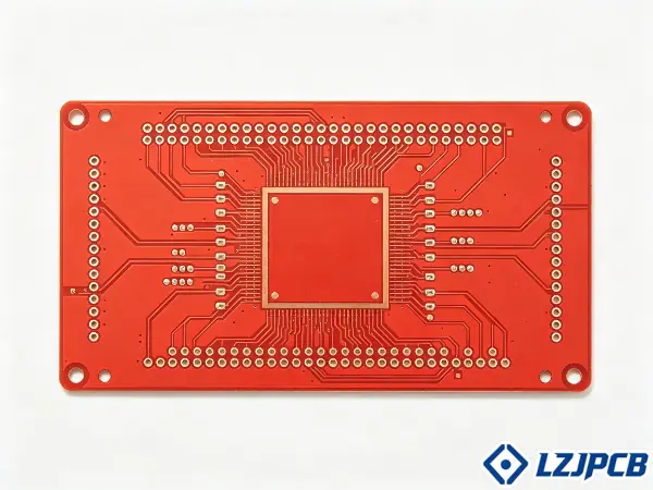
Return path integrity is often more critical than the signal path itself. Yet many designers never think about it. Let me explain why the return current behaves this way and how to keep it clean.
Why Return Current Follows the Signal Trace
At high frequency, return current does not spread across the whole plane. It concentrates directly beneath the signal trace. This is basic electromagnetic behavior.
The current takes the path of lowest impedance, which is the shortest loop area. So it hugs the trace above it. The signal path and the return path together form the full circuit loop.
- Every signal needs an adjacent reference plane to minimize loop area.
- The maximum acceptable loop area gets smaller as frequency rises.
- A small loop radiates little. A large loop radiates a lot.
If you route a high-speed trace over a split in the ground plane, the return current cannot follow. It must detour around the gap. This detour creates a large loop that acts like an antenna. It radiates EMI and degrades the signal. So never route traces over splits, gaps, or voids in the reference plane.
Placing Ground Planes for a Continuous Return Path
To keep the return path continuous, place solid ground planes so every signal trace has an unbroken reference directly below it.
The core rule is simple. Put high-speed signal layers between solid, unbroken ground or power planes. This gives shielding, impedance control, and a clean return path all at once.
Follow these placement rules:
- Never split the ground plane under a signal trace.
- Keep the reference plane solid, with no gaps or voids beneath high-speed nets.
- When a trace changes reference planes, add a via transition to carry the return current across.
- Add ground stitching vias to link ground planes on different layers.
Ground stitching vias provide low-impedance return paths between planes. They cut ground bounce and EMI. Place stitching vias well below λ/20 of your highest frequency, so they contain the fields properly. Routing a high-speed trace from a ground-referenced layer to a power-referenced layer needs careful via design, or the return path breaks at the transition.
Layer Stackup
The wrong stack-up ruins impedance control and creates EMI you can never fix in routing. Stack-up is a prerequisite decision, not a late detail.
A good high frequency layer stackup places high-speed signal layers between solid ground planes, uses a symmetric structure, and references every signal to a continuous ground. Controlled impedance depends on trace geometry, dielectric thickness, and Dk. A change in any single layer alters the impedance of traces referencing that plane.
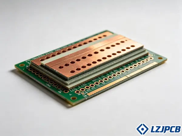
A symmetric, tightly coupled stack-up reduces warpage and gives consistent impedance. This matters more with high frequency laminates, which may expand differently than FR4. Let me cover layer order and reference planes.
Assigning Signal and Ground Layer Order
Layer order decides how well signals are shielded and how clean the return paths are. You assign the order with signal integrity in mind, not just routing convenience.
The main rule is to sandwich high-speed signal layers between solid ground or power planes. This provides three benefits in one move: shielding, impedance control, and a clean return path.
A symmetric stackup helps manufacturing:
- It reduces bow and twist during lamination.
- It keeps impedance consistent across the board.
- It balances copper distribution top to bottom.
Symmetry is not free. Achieving it with certain layer counts forces trade-offs in copper distribution and dielectric arrangement. It may also conflict with layer count limits and cost targets. So evaluate the trade-off per design. Board thickness matters too. Thinner dielectrics make impedance more sensitive to thickness tolerance across production panels. Plan the stackup with your fabricator, not in isolation.
Reference Every High-Speed Layer to Ground
Every high-speed signal layer must sit next to a solid ground reference. This is how you give the return current a clean path and hold impedance steady.
When a signal has a solid ground reference right beside it, the return current flows directly beneath the trace with minimal loop area. This cuts radiation and keeps impedance predictable.
- Reference every high-speed layer to a solid, unbroken ground plane.
- Avoid referencing high-speed signals to power planes unless you add stitching capacitors nearby.
- Use orthogonal routing between adjacent signal layers to reduce broadside coupling.
Route horizontal traces on one layer and vertical on the next. This orthogonal pattern minimizes coupling between adjacent signal layers. Skin effect also matters at high frequency. AC current concentrates near the conductor surface, raising effective resistance roughly with the square root of frequency. Use low-profile or reverse-treated copper foil in your stackup to cut this loss. Smoother copper surfaces mean lower conductor loss.
Trace Routing
Poor routing wastes a good stack-up and good materials. Trace length and spacing decide whether your signals survive the trip.
High frequency trace routing means keeping critical signal traces short and spacing traces far enough apart to reduce crosstalk. Signal radiation scales with routing length. Longer high frequency traces couple more with nearby components. Shorter critical traces cut coupling, radiation, and delay all at once.
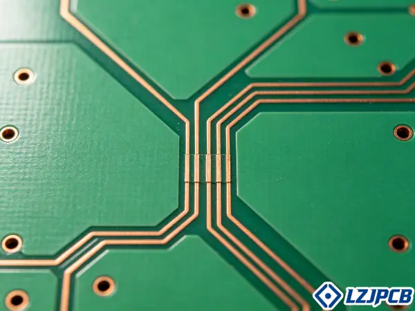
Signal attenuation has two parts: conductor loss from skin effect and dielectric loss from Df. Above 1 GHz, dielectric loss often dominates. Let me cover length and spacing rules.
Keep Critical Signal Traces Short
Short critical traces are a mandatory constraint, not a nice-to-have. Length directly drives radiation and delay.
Clock signals, DDR, USB, Gigabit, and HDMI routing all need short traces. This is required for high frequency designs. Longer traces radiate more and add delay.
A few notes on trace geometry:
- Avoid sharp 90-degree corners. They create local impedance discontinuities and act as capacitive sites.
- Use 45-degree angles or smooth curves instead.
- Wider traces reduce skin-effect resistance at high frequency.
Shortening traces has limits. It is constrained by component placement density and thermal needs. On dense boards, you may not have the space to shorten every path. And a single long critical net can dominate the whole board’s speed classification. So shorten all critical nets, not just some.
For DDR4, use fly-by topology, a form of daisy chain. It reduces the number and length of stubs. This improves signal timing and reliability. Fly-by needs on-die termination and write leveling to handle flight-time skew. That is a deliberate trade-off between signal integrity and layout complexity, and it follows JEDEC design practice.
Set Trace Spacing to Reduce Crosstalk
Trace spacing controls crosstalk. Wider spacing means less coupling between adjacent lines.
The core guideline is the 3W rule. Keep the center-to-center distance between two traces at least three times the trace width. This gives enough physical separation to cut mutual capacitance.
Apply these spacing practices:
- Maximize spacing between different traces during routing.
- Route clock lines perpendicular to signal lines to reduce parallel coupling.
- Minimize parallel run length between adjacent signals.
- Route different signal types on different layers to reduce interference.
Differential pairs need special care. Keep constant spacing between the two traces to preserve consistent differential impedance. Also match their lengths to control skew, since skew causes common-mode conversion and raises EMI. For interfaces like USB, HDMI, and Gigabit Ethernet, hold intra-pair length matching tight. Exact tolerances vary by protocol and data rate. Keep low-voltage differential clocks far from high-frequency clocks, with full attention to reference-plane integrity.
Via Design
Every via you add hurts your signal. Vias are stubs and impedance mismatches rolled into one. At high frequency, via count becomes a real performance variable.
Good via design means using as few vias as possible and adding stitching vias around high-speed signals for shielding. Each via adds about 0.5 pF of parasitic capacitance. This slows signals and raises error probability. So fewer vias means faster, cleaner signals.
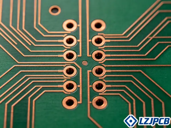
Each via also acts as a stub and an impedance discontinuity at every transition. This is why via strategy matters so much. Let me explain the two sides: cutting vias and adding the right ones.
Why Fewer Vias Improve Signal Integrity
Fewer vias improve signal integrity because each via adds distributed capacitance that limits signal speed. The math is direct. About 0.5 pF per via adds up fast.
More vias mean more cumulative capacitance. That slows the signal and raises the chance of data errors. So there is a trade-off between routing flexibility and signal integrity.
Via stubs make it worse. The unused portion of a via barrel acts as a stub. Stubs cause impedance discontinuities. At high frequency, above a few GHz, they create resonant notches in the transmission response.
To manage vias:
- Keep the via count to a minimum on critical nets.
- Use blind or buried vias to minimize stub length versus through-hole vias.
- Back-drill to remove unused via stubs on high-speed nets.
Back-drilling removes the stub and eliminates the resonant effect. It becomes important above roughly 1 to 5 GHz, depending on stub length. The longer the stub and the higher the frequency, the more it hurts. Set the back-drill depth to remove the unused barrel while keeping the active portion intact.
Add Stitching Vias Around High-Speed Signals
Stitching vias are ground vias placed around high-speed signals to shield them and contain fields. They are the vias you want to add, not remove.
Via fencing places ground vias around signal vias for shielding. This contains the electromagnetic fields and reduces crosstalk to nearby traces.
- Add ground vias along the board edges to contain fields.
- Place stitching vias around high-frequency routing to reduce crosstalk.
- Use stitching vias to link ground planes across layers for a low-impedance return.
Space stitching vias well below λ/20 of your highest frequency of interest. If the spacing is too wide, fields leak between the vias and the shielding fails. When a high-speed signal transitions between reference planes, add stitching vias near the signal via so the return current has a continuous path across the change. Without them, the return current detours and radiates.
Component Placement
Place components poorly and no routing can fix it. Placement locks in your trace lengths before you route a single line.
Good component placement groups high-speed components to shorten traces and places decoupling capacitors right next to power pins. Placement enables or blocks optimal routing. Shorter routing for critical signals requires strategic placement of processors, memory, and connectors before routing begins.
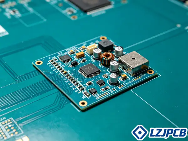
You also must partition the board. Separate RF, analog, digital, and power into distinct physical areas to stop noise coupling. Let me cover decoupling and grouping.
Place Decoupling Capacitors Near Power Pins
Decoupling capacitors must sit as close as physically possible to the IC supply and ground pins. Proximity is as critical as the capacitance value.
The capacitor’s job is to supply transient current and filter high-frequency noise on the power pin. It can only do that if it is close. Distance adds inductance, which kills its effectiveness at high frequency.
- Place high-frequency decoupling capacitors, such as 0.1 µF or smaller, right at the IC power pins.
- Use small, high-quality capacitors for the high-frequency job.
- Keep the loop from the capacitor to the pin as short as possible.
Capacitor effectiveness is frequency-dependent. So target the specific noise frequencies in your design, not just "more capacitance." Match capacitance value, dielectric type, and package to the noise you need to suppress. For designs above 1 GHz, embedded or buried capacitance between plane pairs can lower the power distribution network impedance further. The PDN target impedance must hold across your whole operating bandwidth.
Group High-Speed Components to Shorten Traces
Group high-speed components close together so their connecting traces stay short. This is placement in service of routing.
Components that talk to each other at high speed should sit near each other. Processors, memory, and their connectors form clusters. Short traces between them cut radiation and delay.
Follow these placement rules:
- Group components by signal type.
- Physically isolate radiators like antennas.
- Separate RF, analog, digital, and power sections into distinct areas.
For mixed analog and digital boards, physical partition often beats filtering and grounding alone. Keep digital return currents out of analog ground regions. You can use plane partitioning with controlled bridge points, or moats, which are gaps in the power and ground planes that isolate sections. Apply moats carefully, though. A moat in the wrong place breaks a return path and creates the very problem you tried to avoid.
Grounding and Shielding
Fringing fields and radiated emissions fail EMC tests late in the project. Grounding and shielding contain those fields before they escape.
Good grounding and shielding apply the 20H rule to contain plane-edge fields and add physical shields around high-radiation components. These are EMI containment techniques. The 20H rule recesses the power plane edge relative to the ground plane by about 20 times the inter-plane dielectric spacing.
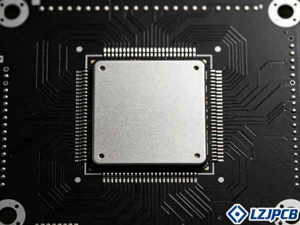
High-frequency boards both emit and absorb EMI. Wireless transmitters and converters radiate noise, while the board can also absorb radiation from nearby devices. Both risks need management. Let me cover the 20H rule and shielding.
Apply the 20H Rule to Reduce Plane Coupling
The 20H rule cuts edge radiation by containing the fringing fields at power plane edges. It recesses the power plane edge inward relative to the ground plane.
The recess distance is about 20 times the inter-plane dielectric spacing, a 20:1 ratio. When the power plane stops short of the ground plane edge by this much, the fringing fields stay contained instead of radiating off the board edge.
- Fringing fields at plane edges radiate as EMI unless you contain them.
- The 20H rule ties recess distance directly to the dielectric spacing between planes.
- It is mainly an EMI containment technique.
I use this rule on almost every high-frequency board. It costs nothing but a small layout change, and it lowers edge radiation measurably. On a design that was failing radiated emissions by a few dB, applying the 20H rule to the power plane helped push it back under the limit.
EMI Shielding Guidelines
EMI shielding physically contains emissions from high-radiation components. Some parts radiate too much to control with layout alone. They need a shield can over them.
For boards with fast-switching circuitry, good filtering is critical to reduce EMI emissions. But apply filtering selectively. Too much filtering on high-speed digital lines degrades rise and fall times and can cause timing violations.
- Add physical shielding over high-radiation components to contain emissions.
- Keep shield openings, like ventilation and connector cutouts, small relative to the wavelength at your highest frequency, often below λ/20.
- Balance shielding against thermal needs, since shields trap heat.
Shielding effectiveness drops at apertures and seams. A large opening lets emissions leak out. When you shield a hot component, add thermal vias or a heat sink, because the shield traps heat. Thermal vias give a conductive path from the hot part to internal or backside copper planes for heat spreading. Choose via diameter and array pitch for effective heat transfer. High frequency materials often conduct heat differently than FR4, so plan cooling early.
Design Verification Before Fabrication
You send the board to fabrication, then find a signal integrity failure on the first prototype. A re-spin costs weeks and money. Verification catches these problems before you commit.
Design verification before fabrication means running signal integrity simulation and checking every design rule against the highest-frequency net. A functional prototype built with correct principles is still different from a mass-producible product. Manufacturability, yield, and consistency separate the two.
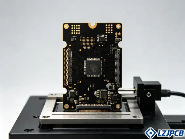
Optimizing a high-frequency PCB layout follows a three-step loop: apply proven guidelines, set up constraints, then verify through rule checks and simulation. The loop is iterative. Failures feed back into constraint adjustments. Let me cover the two verification steps.
Run Signal Integrity Simulation
Signal integrity simulation confirms that your signals stay clean before you build anything. You model the critical nets, vias, and connectors.
Use electromagnetic field solvers to model critical nets, vias, and connectors before you finalize the layout. For demanding high frequency designs, simulation is effectively not optional.
- Simulate signal flow to verify propagation delays, rise times, and crosstalk stay within limits.
- Include near-end and far-end crosstalk analysis for all critical adjacent trace pairs.
- Run PDN simulation to confirm power stays stable under transient loads.
- Add thermal simulation, since higher frequencies often mean higher, localized power dissipation.
Signal integrity simulation needs accurate IBIS or SPICE models for every active component. Missing or wrong models make the results meaningless. PDN simulation must include the frequency-dependent impedance of your decoupling capacitors and plane pairs, so the target impedance holds across the band. Also run an EMC pre-compliance scan, either in simulation or on the bench, to catch radiated emissions before formal certification. This cuts re-spin risk.
Check Design Rules for the Highest Frequency Net
Design rule checking must target the highest frequency net first, because that net has the fastest rise time. Rise time, not just fundamental frequency, sets the harmonic content of a signal.
Faster rise times contain higher-frequency harmonics. Those harmonics worsen ringing, crosstalk, and reflections. So identify the fastest rise-time signals early and treat them as your primary monitoring targets.
Run these checks:
- Identify the top frequency net and the maximum rise time before layout begins.
- Verify electrical specs at both the source and the sink, since passing at the driver does not guarantee compliance at the receiver.
- Run post-route DRC for differential pair phase tolerance, maximum stub length, and via count per net.
- Confirm all selections fall within the contract manufacturer’s DFM capabilities.
This is where our approach at LZJPCB helps our clients most. Our engineers work with your team during the design phase, not just at order time. We check that your stackup, impedance targets, and via geometries fit our manufacturing capabilities before you commit. I have caught many issues at this stage that would have cost a client a full re-spin. Plan your stackup with your fabricator, confirm achievable impedance tolerances, and verify drilling capabilities for complex vias. A design rule that exceeds the CM’s minimum trace width or aspect ratio is not producible, no matter how good the simulation looks.
FAQs About High Frequency PCB Design
What frequency counts as high frequency for a PCB?
A PCB counts as high frequency at 100 MHz and above, reaching into the gigahertz range. For RF signals, effects can appear around 50 MHz. Critical design rules change fundamentally above 1 GHz.
Can I use FR4 for a high frequency PCB?
FR4 works below a few GHz with care, but it becomes unreliable above that. Its Dk drifts with frequency and its high Df causes signal loss. Use Rogers RO4350B, Isola Astra, or Panasonic Megtron 6 for demanding designs.
Why does my high frequency signal reflect?
Signals reflect at any impedance discontinuity, such as a via, a connector pad, or a sharp trace angle. Match the source, trace, and load impedance across the whole path, typically 50Ω single-ended or 100Ω differential.
How do I reduce crosstalk on a high frequency board?
Apply the 3W rule, keeping trace center-to-center spacing at least three times the trace width. Route clock lines perpendicular to other signals, add ground planes and stitching vias, and shorten parallel run lengths.
Do I need to back-drill vias?
Back-drill vias when stubs cause signal integrity problems, generally above 1 to 5 GHz depending on stub length. Back-drilling removes the unused via barrel and eliminates the resonant stub effect. Blind or buried vias also reduce stub length.
Conclusion
High frequency PCB design demands low-loss materials, tight impedance control, continuous return paths, and clean partitioning. Verify with simulation and DFM before you build.