

Your ADAS board fails one thermal cycle, and a safety-critical car system goes dark. The risk is real. The fix starts with the right PCB.
An ADAS domain controller PCB is a centralized high-speed computing board that fuses camera, radar, lidar, and Ethernet data in real time. It uses HDI multilayer construction, tight impedance control, automotive-grade materials, and ISO 26262 safety design to support powerful SoCs and AI accelerators.
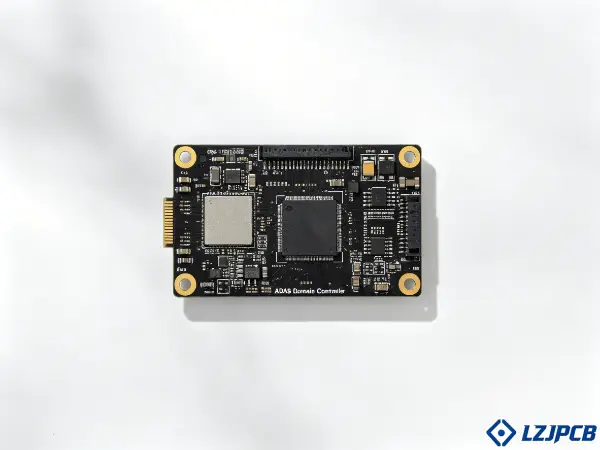
I have built ADAS boards for Europe and japan clients. Each one taught me something new. Let me walk you through what really matters, from design to procurement.
What Is an ADAS Domain Controller PCB?
Modern cars used to scatter dozens of ECUs across the chassis. That mess slowed everything down. The domain controller fixed it by putting one brain in charge.
An ADAS domain controller PCB is a centralized computing board that integrates multiple vehicle ECUs into one high-performance unit for sensor fusion and real-time decision-making. It fuses camera, radar, lidar, and Ethernet data and runs advanced SoCs like NVIDIA Orin, Mobileye, or Renesas R-Car.
These boards act as the car’s central brain. They replace old distributed ECUs with one tight, powerful unit. That shift speeds up response time, but also makes the PCB far more complex. Below I break down the three things that define this board.
Core Functions of ADAS Domain Controller PCB
The core job is sensor fusion. The board takes raw data from cameras, radar, and lidar, then merges it into one clear picture of the road. This happens in real time. A delay of milliseconds can mean a missed obstacle.
To do this work, the board carries advanced SoCs such as NVIDIA DRIVE, Mobileye, or Renesas R-Car. These chips need a complex high-speed signal integrity design on the PCB. They also need clean power and fast memory access.
Here are the main functions I designed for:
- Fuse camera, radar, lidar, and Ethernet data in real time
- Run AI inference for object detection and path planning
- Route data between zone ECUs over Automotive Ethernet
- Handle redundant safety paths for fault tolerance
- Manage multi-rail power for the main compute load
Each function adds routing density. That is why these boards almost always use HDI construction. The board must pack thousands of connections into a small space, It must also keep every signal clean. I treat the layout as a system, not a flat drawing.
High-Speed Signal Integrity in ADAS PCB
High-speed signals are the heart of these boards. Interfaces like PCIe Gen4/Gen5, MIPI CSI-2, and Automotive Ethernet move multi-gigabit data. A small layout error can corrupt that data and break the whole system.
These interfaces need very tight impedance control, length matching, and low-loss routing. Domain controller SoCs often need impedance held to ±5%. Camera links need 100Ω differential pairs with skew under 5 mils. I also use back-drilling to remove via stubs that hurt signal quality.
| Interface | Typical Speed | Key Design Rule |
|---|---|---|
| PCIe Gen4/Gen5 | 16–32 GT/s | ±5% impedance, back-drilling |
| MIPI CSI-2 | Multi-gigabit | Low-loss material, length match |
| 1000BASE-T1 Ethernet | 1 Gbps | Return loss control, EMI suppression |
| CAN FD / FlexRay | Lower speed | Clean grounding, isolation |
Note one thing. Automotive Ethernet such as 100BASE-T1 and 1000BASE-T1 are true high-speed link. CAN FD and FlexRay are not high-speed in the SerDes sense, but they still ride on the same board. I keep them on separate domains. Clean domain separation stops noise from crossing over. That is the only way to keep gigabit links stable next to radar and power electronics.
Thermal Management Challenges in ADAS PCB Design
Heat is the enemy here. High-performance SoCs and AI accelerators burn hundreds of watts in a tight space. If that heat stays in the board, the chip throttles or fails. I have seen boards crack at the via under repeated heat stress.
So thermal management drives many layout choices. I use heavy copper layers, thermal via arrays, and heat spreaders to pull heat away from the hot parts. For extreme heat, I embed a copper coin right under the SoC. That gives a direct, low-resistance path to the heatsink.
Here is how I plan thermal design, step by step:
- Map the power and heat of every major chip first
- Place thermal via arrays under each high-power BGA
- Add 2oz or heavier copper on internal power planes
- Use a copper coin or metal core for the hottest parts
- Keep the stackup symmetrical to stop warping
- Validate with thermal cycling before production
Symmetry matters more than people think. An unbalanced stackup warps during reflow and under road heat, which breaks solder joints over time. I keep copper balanced from the center core out. This small habit saves boards from early failure.
ADAS Domain Controller PCB Specifications
Spec sheets look boring until one wrong number kills your project. A loose impedance tolerance or a weak laminate ruins reliability. The details decide everything.
ADAS domain controller PCBs typically use 12 to 20+ layer HDI construction with high-Tg, low-CTE laminates, blind and buried vias, and impedance control held to ±5% for high-speed interfaces. They meet IPC-6012DA automotive criteria for via plating and thermal cycling survival.
I always start a project by locking the specs with the client. Guessing here costs money later. Let me explain the three specs that matter most for these boards.
Layer Count and Build-Up for ADAS PCB Reliability
A domain controller cannot fit on a 6 or 8-layer board, cause routing is too dense. Most of these boards need 12 to 20+ layers and heavy HDI use. The fine pitch of AI processors, often 0.5mm or 0.6mm BGA, forces this density.
I pick the build-up based on routing needs. Simpler boards use sequential build-up (SBU) for 6 to 10 layers. Complex sensor-fusion boards use every-layer interconnect (ELIC) for 12+ layers. ELIC gives the most routing freedom but costs more.
Our PCB factory supports HDI types of 1+N+1, 2+N+2, and 3+N+3, with up to 32 layers in mass production. I lean on this range to match cost and density. The key is to use just enough HDI to route the board cleanly. Overbuilding wastes money, and underbuilding forces ugly compromises in routing. I always model the stackup first, then confirm it with the fab before layout starts. This step alone prevents most reliability surprises down the line.
Dielectric Materials for ADAS Domain Controller PCB
The dielectric layer sets the base for both speed and reliability. For domain controllers, I use high-Tg, low-CTE laminates with stable dielectric properties across temperature and humidity. A Tg of 170°C or higher is the floor for automotive use.
The material must hold its dielectric constant steady across the full temperature range. If Dk drifts, impedance drifts, and signals degrade. That is why I avoid cheap FR4 on the high-speed layers. I use controlled, traceable laminates instead.
| Property | Target Value | Why It Matters |
|---|---|---|
| Tg (glass transition) | ≥170°C | Survives reflow and road heat |
| CTE | Low, matched | Stops via cracking under cycling |
| Dk stability | Tight over temp | Keeps impedance steady |
| Df (loss) | ≤0.005 for high-speed | Cuts insertion loss |
Our factory stocks A-grade laminates from Shengyi, KB, and Jinguo, all UL- and RoHS-traceable. We also run high-Tg, Rogers, halogen-free, and hybrid stacks. I match the material to the exact interface speed and the car’s service life. The right laminate is the cheapest insurance you can buy.
Impedance Control Tolerances for ADAS PCB
Impedance control is where many boards fail in silence. The board looks fine, but the signals are weak. For domain controller SoCs, I hold impedance to ±5%. For the camera and many digital links, ±10% can work.
I reach this tolerance with careful trace width, spacing, and stackup control. Our standard impedance control is ±5%, which matches what these boards need. I also design proper test coupons so the fab can prove the impedance on every panel.
Here is my impedance checklist:
- Define target impedance per net class before layout
- Set ±5% for PCIe, Ethernet, and SoC links
- Keep continuous reference planes under every high-speed trace
- Match intra-pair skew under 5 mils
- Add impedance test coupons to the panel
- Confirm with TDR on the first build
The reference plane rule is the one people break most. A signal that crosses a split plane loses its return path, which creates EMI and weak signals. I never let a high-speed trace cross a gap. This single rule saves more boards than any other.
How to Choose Materials for ADAS Domain Controller PCB
Pick the wrong material and your board fails in the field, not the lab. By then it is too late and too costly. Material choice is a make-or-break call.
Choose materials for ADAS domain controller PCBs based on three things: low-Dk and low-Df for high-frequency signals, CTE matching to survive thermal cycling, and halogen-free options for safety and compliance. Match each property to the board’s speed, heat load, and service life.
I treat material choice as the first real design decision. It shapes cost, speed, and reliability all at once. Here is how I think through the three big trade-offs.
Low-Dk and Low-Df Materials for High-Frequency ADAS PCB
High-frequency signals lose energy in the dielectric. The loss factor, Df, controls how much. For high-speed routing, I use materials with a Df of 0.005 or less. A low Dk also keeps signals fast and impedance stable.
Standard FR4 has high loss. It absorbs fast signals and weakens them. So for PCIe Gen5, multi-gig Ethernet, and MIPI links, I move to low-loss laminates. Sometimes I use a hybrid stack, mixing a low-loss material on the high-speed layers with FR4 on the slower layers.
Here is how I rank materials by need:
- Low-loss laminate (Df ≤0.005): high-speed SerDes and SoC links
- High-Tg FR4 variant: power planes and slower digital
- Hybrid stack: best cost-to-performance balance
- Rogers or PTFE: only when RF or mmWave is on-board
Our factory runs Rogers, PTFE, Nelco, and hybrid material stacks, so I can mix them in one board. The goal is to spend on low-loss material only where the speed demands it. This keeps costs in check while protecting the critical signals. I always confirm the loss budget with simulation before I lock the stack.
CTE Matching in ADAS PCB
CTE is the coefficient of thermal expansion, which tells you how much a material grows when it heats up. If the laminate and the copper grow at different rates, the via cracks. That is a top failure mode in automotive boards.
ADAS boards cycle from -40°C to 125°C, often for 1000 cycles or more. Each cycle stresses the vias and the laminate bond. So I pick low-CTE laminates that match the copper and the component packages. This keeps the board stable across the full temperature range.
CTE matching matters most in the Z-axis, through the thickness of the board. High Z-axis expansion pulls on plated through-holes and microvias. I use low-CTE, high-Tg material to limit this. I also keep the stackup symmetrical so the board does not warp.
For the SoC area, I match the board CTE to the BGA package as closely as I can. A big mismatch under a large BGA breaks solder joints over time. This is the kind of slow failure that ruins a product’s reputation. I would rather pay more for the right laminate than face field returns. Good CTE matching is quiet, invisible work that pays off for years.
Halogen-Free vs Halogenated Materials for ADAS PCB
Halogen-free materials remove bromine and chlorine compounds. This matters for safety and environmental rules. Many carmakers now require halogen-free boards. Burning halogenated material releases toxic fumes, which is a real concern in a vehicle.
Here is the trade-off I weigh:
| Factor | Halogen-Free | Halogenated |
|---|---|---|
| Safety in fire | Lower toxic smoke | Higher toxic smoke |
| Compliance | Meets strict OEM rules | May not pass |
| Cost | Slightly higher | Lower |
| Thermal stability | Often very good | Good |
| Availability | Growing fast | Wide |
For ADAS domain controllers, I lean toward halogen-free where the OEM allows it. The safety case is strong, and many of our clients in Europe require it. Our factory stocks halogen-free laminates, and they are RoHS and REACH traceable, with SVHC reports on hand.
That said, I do not force halogen-free if it hurts performance or breaks the budget without need. I check the OEM spec first. Then I match the material to both the rule and the electrical need. The right choice depends on the customer and the market the car will sell in.
ADAS PCB Cost Drivers: From Prototype to Production
Sticker shock on an ADAS quote is common. The price jumps for reasons buyers cannot see. If you do not know the drivers, you overpay or cut the wrong corner.
The main cost drivers for ADAS domain controller PCBs are layer count, panel utilization, surface finish, and order volume. HDI build-up and high layer counts raise price the most, while smart panel use and the right finish keep costs under control.
I help clients see where the money goes before they commit. A clear cost map lets you choose wisely. Let me break down the three drivers I watch most.
How Layer Count and Panel Utilization Affect ADAS PCB Pricing
Layer count is the biggest single driver. Each added layer adds material, lamination, and process steps. HDI build-up adds even more, since each microvia layer means a laser-drill and plate cycle. A 20-layer ELIC board costs far more than a 12-layer SBU board.
Panel utilization is the hidden lever. Your board has to fit on a standard production panel. If your board size wastes panel space, you pay for that wasted material. I always check panel fit early. A small size tweak can fit more boards per panel and drop the unit price a lot.
Here is how I cut the layer and panel cost:
- Use just enough HDI to route the board, not more
- Pick SBU over ELIC when density allows
- Adjust board outline to improve panel fit
- Combine small boards into one panel array
- Lock the stackup before layout to avoid rework
Our factory runs panels up to 650×2000mm, which gives me room to optimize the array. I model both layer count and panel fit at quote time. This early work often saves clients 10 to 20 percent. The cheapest savings come from planning, not from cutting quality.
Surface Finish Cost Implications for ADAS PCB
Surface finish protects the copper pads and sets the solder quality. For ADAS boards with fine-pitch BGAs, the finish matters a lot. A flat, even finish gives reliable solder joints. A poor finish causes opens and shorts under the BGA.
ENIG is my default for these boards. It gives a flat surface for fine-pitch parts and resists corrosion. It costs more than HASL but works far better for dense SoC packages. For some boards, I use ENIG+OSP or immersion silver to balance cost and performance.
| Finish | Cost | Best Use on ADAS PCB |
|---|---|---|
| ENIG | Higher | Fine-pitch BGA, long life |
| Immersion silver | Medium | High-speed, flat surface |
| Lead-free HASL | Lower | Larger pads, lower cost |
| ENIG+OSP | Higher | Mixed pad types |
Our factory runs all of these, plus electroplated gold and gold fingers. I match the finish to the smallest pitch on the board. A 0.3mm pitch BGA needs ENIG or better. There is no point in saving on finish if the SoC will not solder correctly. I treat the finish as part of the reliability plan, not just a cost line.
MOQ Considerations for ADAS Domain Controller PCB
MOQ stands for minimum order quantity. It shapes your cost at every stage. For prototypes, a high MOQ wastes money on boards you do not need yet. For production, a low MOQ raises the unit price.
I structured the order to match the project phase. In the prototype stage, I support small builds with no forced minimum. This lets clients test the design before they commit to volume. Our component team also supports prototyping with no minimum order quantity, so we can kit small runs fast.
Here is how I plan order volume across the project:
- Prototype: small build, no MOQ, fast turn
- Validation: small batch to confirm reliability
- Pilot: mid-volume to test the supply chain
- Production: full volume for the best unit price
The jump from prototype to production is where flexibility pays off. Many clients need to serve different markets at different volumes. I have factories in China and Indonesia, so I can scale up or shift production to match. This lets a client like a German buyer ramp volume without locking into one rigid line. The right MOQ plan protects both cash flow and lead time.
5 Certifications Every ADAS PCB Supplier Must Hold
A missing certification can sink your whole program. OEMs will reject an uncertified supplier on sight. The wrong partner wastes months that you cannot get back.
Every ADAS PCB supplier must hold IATF 16949 for automotive quality, build to IPC Class 3 for high-reliability assembly, and prove reliability through thermal cycling and HAST testing. ISO 26262 functional safety awareness and IPC-6012DA fabrication standards are also essential.
I tell every client to check certs before anything else. They are the price of entry for automotive work. Let me explain the three that matter most for a domain controller board.
IATF 16949 for ADAS PCB
IATF 16949 is the automotive quality management standard. It requires full traceability of materials and processes. For ADAS work, this is not optional. A board failure can be fatal, so the OEM must trust every step of your process.
This standard forces a real quality system, not just inspection at the end. It covers supplier control, process control, and corrective action. When I source for a client, I confirm the fab holds a current IATF 16949 certificate before I quote.
Our factory earned IATF 16949 certification in 2023. We back it with ISO9001, ISO14001, and ISO13485 for medical work. This means I can give a German automotive buyer the traceability they need. Every laminate, every process, every test is logged. That paper trail is what lets a buyer pass their own OEM audit. Without it, the door to automotive work stays closed.
IPC Class 3 vs Class 2 for ADAS Domain Controllers
IPC Class sets the acceptance standard for the assembly. Class 2 is for general electronics. Class 3 is for high-reliability products where failure is not an option. ADAS domain controllers need Class 3.
The difference shows up in the details. Class 3 demands tighter tolerances on solder joints, annular rings, and via fill, It allows fewer defects, also requires more inspection. For a safety-critical board, those tighter rules are worth it.
| Criteria | IPC Class 2 | IPC Class 3 |
|---|---|---|
| Target use | General electronics | High-reliability, safety-critical |
| Solder joint rules | Standard | Tighter, fewer defects |
| Annular ring | More relaxed | Strict minimums |
| Inspection level | Normal | High, full coverage |
| ADAS fit | Not enough | Required |
Automotive-grade PCB manufacturing typically requires IPC Class 3 assembly standards for long-term reliability in harsh driving environments. I always build ADAS boards to Class 3. Our SMT lines use 3D SPI, inline AOI, and X-Ray to hit that standard. The extra inspection catches the hidden faults that Class 2 might miss. For a car system, that margin is the whole point.
Reliability Testing: Thermal Cycling and HAST for ADAS PCB
Reliability testing proves the board survives the field. Two tests matter most: thermal cycling and HAST. Thermal cycling runs the board from -40°C to 125°C for 1000+ cycles. This finds via cracks and delamination before the car ships.
HAST stands for Highly Accelerated Stress Test. It uses high heat and humidity under pressure to age the board fast. It exposes weak insulation and migration risks in days, not years. Together these tests model the harsh life of an ADAS board.
Here is the reliability test flow I run before production release:
- Thermal cycling: -40°C to 125°C, 1000+ cycles
- HAST: high temp and humidity under pressure
- Vibration: simulate road and engine stress
- TDR and VNA: confirm impedance and signal integrity
- Microsection: check via plating and lamination
A good ADAS supplier should support power-integrity validation, signal-integrity verification, and thermal and mechanical reliability testing before production release. I treat these tests as a gate. No board ships to volume until it passes. This is how I catch failures like via cracking and delamination early, instead of in the customer’s car.
ADAS PCB Procurement: 4 Mistakes That Delay Production
A delayed ADAS board stalls the whole car program. Each lost week costs real money. Most delays trace back to a few avoidable mistakes in procurement.
The four mistakes that delay ADAS PCB production are poor impedance test coupon design, material lead time misalignment, weak warpage control on large boards, and skipping early DFM review. Catching these at the quote stage keeps production on schedule.
I have seen these mistakes stall projects again and again. The good news is they are all preventable. Let me show you the three I see most and how I avoid them.
Impedance Test Coupon Design Oversights in ADAS PCB
The impedance test coupon proves your board hits the target impedance. It is a small test strip on the panel. If the coupon is wrong or missing, the fab cannot verify impedance. That stops the build or forces a re-spin.
Many designs treat the coupon as an afterthought. That is a mistake. The coupon must match the real stackup and the real net classes. It must include the trace widths the fab needs to measure. I design the coupon with the board, not after.
Here is my coupon checklist:
- Include one coupon per controlled-impedance layer
- Match the coupon trace width to the real design
- Cover both single-ended and differential nets
- Place coupons in the panel border, not the board
- Confirm the fab can probe them with TDR
I make sure every ADAS board has a clean, complete coupon set. This lets the fab prove ±5% impedance on every panel. It also gives the client a record for their own audit. A good coupon is cheap. A missing one can cost weeks of delay and a full re-spin. I never skip this step.
Material Lead Time Misalignment With ADAS PCB Production
Special materials have long lead times. Low-loss laminates, Rogers, and high-Tg stocks can take weeks to arrive. If you do not order them early, the whole build waits. This is one of the most common causes of delay I see.
The fix is to align material lead time with the production plan from day one. I check material stock and lead time at the quote stage. If a laminate is long-lead, I order it before the design is final. This parallel approach saves weeks.
Here is how I keep materials on track:
- Identify all special materials at quote time
- Check stock and lead time before design freeze
- Pre-order long-lead laminates in parallel
- Hold safety stock for repeat production
- Confirm laminate batch traceability for IATF
Our factory stocks A-grade laminates from Shengyi, KB, and Jinguo, plus Rogers and hybrid materials. This buffer lets me start many builds without a long wait. For repeat orders, I keep safety stock so production never stalls on material. Planning the material timeline is dull work, but it is the difference between on time and late.
Warpage Control for Large ADAS PCB
ADAS domain controller boards are big and thick. Big boards warp. Warpage breaks solder joints, fails fine-pitch BGAs, and jams the assembly line. For a board with thousands of BGA pins, even a small warp is a problem.
I control warpage through stackup design and process control. The key is a symmetrical stackup, with balanced copper from the center core out. An unbalanced board warps during reflow and under heat. I also pick low-CTE material to limit movement.
Here is my warpage control plan:
- Design a symmetrical, balanced stackup
- Balance copper across all layers
- Use low-CTE, high-Tg laminate
- Add support or stiffeners for very large boards
- Measure warpage on the first build before volume
Our factory handles boards up to 650×2000mm with ovens and laminators built for large panels. I run a warpage check on the first article before I release volume. This catches a warping board before it ruins a full production run. For large, dense ADAS boards, warpage control is not a detail. It is core to a clean assembly yield.
LZJPCB supports ADAS domain controller PCB projects end-to-end. We handle HDI fabrication, multilayer high-speed PCB production, SMT assembly, component sourcing, and scalable automotive-grade production across our factories in China and Indonesia. With our IATF 16949 process, dedicated engineers, and turnkey service, I help global buyers solve slow delivery and hard procurement on complex boards.
Conclusion
ADAS domain controller PCBs demand HDI density, tight impedance, automotive materials, and full certification. Choose a partner like LZJPCB with proven automotive-grade capability, and your production stays on track.