Skip to content
The main disadvantages of SMT are limited power handling, difficult rework, weaker solder joints under thermal stress, the need for hidden-joint inspection, and high setup costs that hurt small batches. SMT parts are smaller than through-hole parts and often have no leads, so they pack tightly but bond weakly and depend on precise equipment.
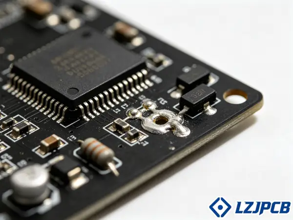
I have led more than 300 PCB assembly projects over 7 years. I have seen every SMT assembly weakness listed here fail a real board. Below I break down each one, so you can decide with clear eyes.
Limited Power Handling Capacity
A power SMD looks fine until it runs hot. Then the joint heats, the solder softens, and the part drifts. Power limits are the first SMT trap.
SMT handles less power than through-hole because small parts dissipate heat poorly and small solder joints carry limited current. A typical SMT pin carries about 1–2A, while a through-hole lead can carry 5–10A. Heavy power parts still belong in through-hole.
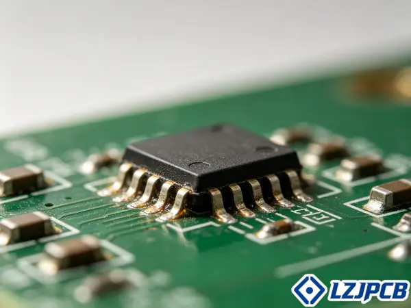
I always split high-power designs. My team uses SMT for control logic and through-hole for MOSFETs and transformers. This hybrid choice keeps the board reliable under load.
Heat dissipation limits of small components
Small SMT parts have small bodies. A small body has a small surface area. A small surface area dissipates less heat. This is simple physics, and it sets a hard limit on power.
Some people claim SMT always dissipates less heat than through-hole. That is not true. Heat dissipation depends on the part and the design, not the mount type. Power SMDs like D²PAK and TO-263 use thermal pads to sink heat into the board.
A standard SOIC-8 has a junction-to-ambient thermal resistance near 100–150°C/W. A DIP package sits lower, near 60–80°C/W. So a bare SMT chip runs hotter for the same power.
To fix this, I use these steps:
- Add thermal vias under the part to move heat into inner copper.
- Extend copper pads to spread heat across the board.
- Use aluminum-core PCBs for high-power LED or driver boards.
- Pick parts rated for 150°C or higher in hot enclosures.
Without these steps, a power SMD can overheat and fail early. Good thermal design turns a weak point into a manageable one.
Current limits of solder joints
An SMT solder joint is tiny. It holds a small volume of solder, often 0.5–2mg per connection. A through-hole joint holds far more, near 10–50mg. Less solder means less metal to carry current.
This limits current per pin. For high current, one pin is not enough. So designers spread current across many pins or copper planes. That works, but it costs board space and adds design effort.
I once reviewed a motor drive board where the client pushed too much current through a single SMT pad. The pad lifted after weeks of use. We moved that path to a through-hole terminal, and the failures stopped.
Here is a quick comparison I share with clients:
| Factor | SMT joint | Through-hole joint |
|---|---|---|
| Solder volume | 0.5–2mg | 10–50mg |
| Current per pin | ~1–2A | ~5–10A |
| Best use | Signal, low power | Power, high current |
The lesson is clear. Match the mount type to the current. SMT for signals, through-hole for real power paths.
Rework and Repair Difficulty
A failed SMT part is hard to remove. Parts sit close together. Heat spreads to neighbors. One wrong move damages the board. Rework is a real SMT pain point.
SMT rework is harder than through-hole because parts are tiny, packed tightly, and need hot-air stations instead of a simple iron. SMT rework costs about 3–5 times more than through-hole rework for the same part count, and a pro rework station costs $5,000–$20,000.
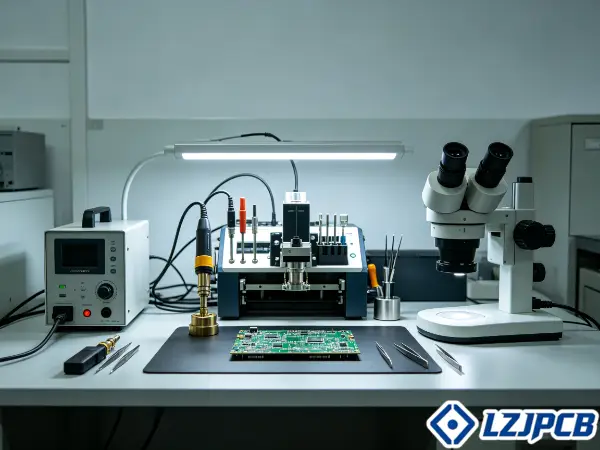
I train my team on rework limits. We allow no more than three reflow cycles on the same pad. Past that, the pad weakens and the joint gets unreliable. Repair has a budget too.
Equipment required for rework
You cannot fix most SMT boards with a basic iron. You need proper tools. Small parts and hidden joints demand controlled heat and steady hands.
A standard SMT rework setup includes:
- Hot-air rework station with temperature-controlled nozzles.
- Bottom-side preheater to stop board warpage.
- Fine-tipped iron for two-terminal parts.
- Microscope for placement and inspection.
- Stencil or dispenser for fresh solder paste.
For a BGA, the process runs step by step: pre-bake the board, remove the part with hot air, clean the pads, print fresh paste, place the new part, then reflow. Each step needs skill and the right gear.
Compare this to DIP. A DIP part needs a $10–$50 iron. You desolder, pull the part, drop in a new one, and resolder in about five minutes. That gap explains why schools and R&D labs still love DIP. Accessibility matters when you fix boards by hand.
Risk of pad damage during removal
Every rework cycle adds heat to the board. Heat weakens the bond between the copper pad and the laminate. Too much heat lifts the pad off the board. A lifted pad often means a dead board.
Dense layouts make this worse. Parts sit so close that heating one part heats its neighbors. A nearby part can shift or reflow by accident. So skilled operators shield neighbors and control the heat window tightly.
I follow IPC-7711 and IPC-7721 for rework. These standards set clear limits and methods. After rework, we check the joint with X-ray or a cross-section for critical boards.
The key risks during removal are:
- Pad lifting from too much heat or too many cycles.
- Adjacent parts moving under stray hot air.
- Cold joints from rushed reflow.
- Pad cratering under BGA corners.
Because of these risks, I tell clients to design for repair. Leave clearance around large parts. Avoid placing critical parts near board edges. Good layout makes rework safer and cheaper.
Solder Joint Reliability Under Thermal Stress
An SMT joint holds through room temperature. Then the board heats and cools, day after day. The joint flexes each cycle. Over time, it cracks. Thermal stress is a silent SMT killer.
SMT solder joints fail under thermal stress because the part and the board expand at different rates, and small joints fatigue faster during temperature cycling. Automotive boards face -40°C to +125°C cycles, and mature SMT joints must survive 1,000–5,000 cycles per IPC-9701.
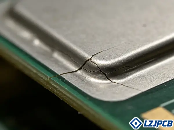
I design for reliability from day one. For BGAs in harsh use, I add underfill. For automotive work, I follow IPC-9701 test ranges. Reliability is a design choice, not luck.
CTE mismatch between component and board
CTE means coefficient of thermal expansion. It tells how much a material grows when it heats. A part and the board grow by different amounts. That difference pulls on the joint between them.
A ceramic MLCC capacitor has a CTE near 6 ppm/°C. An FR-4 board has a CTE near 14–17 ppm/°C in the X-Y plane. When the board cools, it shrinks more than the ceramic part. This puts stress on the joint, sometimes 20–40 MPa, enough to crack ceramic in extreme cases.
Here is the mismatch that causes trouble:
| Material | CTE (ppm/°C) |
|---|---|
| Ceramic (MLCC) | ~6 |
| FR-4 board (X-Y) | ~14–17 |
This mismatch matters most for large ceramic parts on standard boards. To manage it, I do the following:
- Orient parts to reduce flex stress along the weak axis.
- Use flexible-termination MLCCs in high-stress spots.
- Add underfill under large BGAs to spread the load.
- Match materials better in extreme-temperature designs.
The mismatch never goes away. But good part choice and layout keep it below the danger line.
Thermal cycling fatigue in joints
Fatigue means damage from repeated stress. A joint that survives one cycle can still fail after thousands. Each heat-cool swing bends the joint a little. Small cracks grow until the joint opens.
SMT joints fatigue faster than through-hole joints because they hold less solder. There is less metal to absorb the strain. Void formation makes this worse, since voids weaken the joint from inside.
I test critical boards against IPC-9701 cycling and JEDEC shock standards like JESD22-B111. For handheld products, I also run drop tests. These tests reveal weak joints before the client’s customer does.
Common failure modes I watch for include:
- Solder fatigue cracks from thermal cycling.
- Voids from outgassing during reflow.
- Head-in-pillow defects on BGA balls.
- Intermetallic growth that makes joints brittle.
To fight fatigue, I optimize the reflow profile, use low-voiding solder paste, and add mechanical support where needed. A mature SMT process can hold defects below 50 ppm. That level takes real process control, not just good parts.
Inspection Challenges for Hidden Joints
Some SMT joints hide under the part. You cannot see them. You cannot probe them easily. A hidden defect passes visual checks and fails in the field. Inspection is a core SMT challenge.
SMT inspection is hard because BGA and QFN joints hide under the part, so you cannot judge them by eye and must use X-ray. Fine-pitch parts below 0.5mm and all BGAs need AOI or X-ray, which adds cost and time to every board.
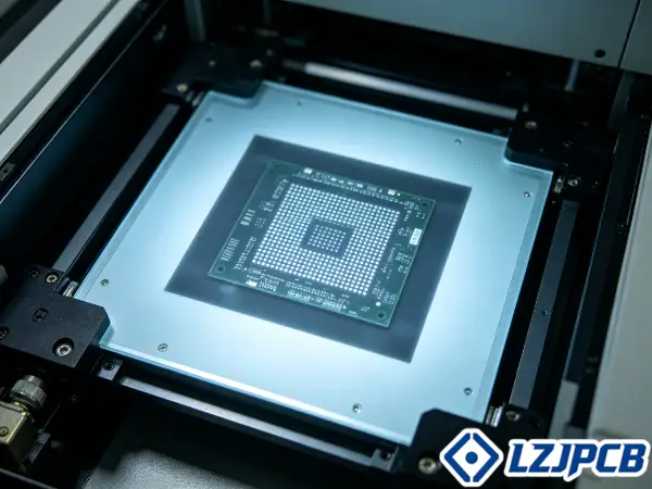
I never ship a BGA board without X-ray. My factories run AOI on visible joints and X-ray on hidden ones. Inspection is not optional for high-reliability work.
X-ray inspection required for BGA and QFN
A BGA hides its solder balls under the chip. A QFN hides its pad under the body. No camera can see these joints from the side. Only X-ray sees through the part to the joint.
X-ray inspection, also called AXI, checks hidden joints for shorts, voids, and open connections. It is standard for every BGA, not just fine-pitch ones. The joints stay hidden no matter the ball spacing.
My inspection stack looks like this:
- SPI checks solder paste volume and alignment before placement.
- AOI checks visible joints after reflow at 95–99% detection.
- AXI checks hidden BGA and QFN joints with X-ray.
- ICT verifies electrical function on production boards.
Each layer catches different defects. X-ray adds cost and time, but it is the only way to trust a hidden joint. For BGAs with balls below 0.5mm, this becomes non-negotiable.
Visual inspection cannot see under components
Visual inspection works on parts with visible leads. You look at the joint, judge the shape, and pass or fail. But a BGA has no visible leads. The joints sit under the body, out of sight.
So visual checks miss hidden defects entirely. A bad ball can pass a visual pass and still cause a field failure. This is the core limit of eye-based inspection for modern packages.
The small size of SMT parts makes this worse. Dense layouts crowd the view. Solder bridges hide between fine-pitch pins. A tombstoned part can look fine from one angle. Human error climbs fast without automation.
Because of this, I rely on layered inspection:
- SPI before reflow to catch paste problems early.
- AOI to catch visible bridges, misalignment, and tombstones.
- AXI to catch what no camera can reach.
The takeaway is simple. For any board with hidden joints, plan for X-ray from the start. Visual inspection alone is not enough. Skipping this step trades a small cost now for a big field failure later.
Higher Setup and Equipment Costs
SMT looks cheap per unit. Then you price the line. Printers, placement machines, ovens, and inspection all cost money. High setup cost is the SMT barrier for small players.
SMT setup costs far more than through-hole because it needs pick-and-place machines, reflow ovens, stencils, and AOI systems. A full SMT line runs over $1 million, while a through-hole line starts near $70,000.
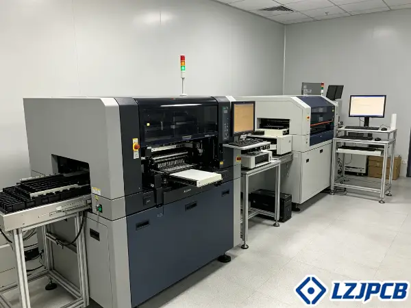
I invested in three PCBA factories to build this capacity. The upside is speed and consistency. The downside is a high entry cost that only makes sense at volume.
Stencil and pick-and-place machine costs
Every SMT job starts with a stencil. A laser-cut stencil costs $3–$43. It prints solder paste onto the pads. You need a new stencil for each board design, so each new product carries this fixed cost.
The pick-and-place machine places the parts. Modern machines place 20,000 to over 100,000 parts per hour. That speed is the real SMT advantage at volume. But the machine costs hundreds of thousands of dollars and needs skilled setup.
The main upfront SMT costs are:
- Stencil tooling: $3–$43 per design.
- Solder paste printer with alignment.
- Pick-and-place machine with feeders.
- Programming and first-article setup time.
For a prototype run, these fixed costs dominate. Spread across ten boards, the cost per board is huge. Spread across ten thousand, it nearly vanishes. Volume is what makes SMT pay off.
Reflow oven and AOI system investment
The reflow oven melts the paste and forms the joints. A good oven has 10 to 12 heat zones and nitrogen capability. It needs a precise temperature profile with ramp rates near 1–3°C per second and a peak near 235–245°C for lead-free solder.
The AOI system inspects the finished joints. It catches bridges, missing parts, and misalignment at high speed. Both the oven and the AOI cost serious money, and both need trained staff to run well.
Here is a rough cost picture I share with clients:
| Equipment | Rough cost |
|---|---|
| Solder paste printer | $30k–$150k |
| Pick-and-place machine | $100k–$500k+ |
| Reflow oven | $50k–$200k |
| AOI system | $50k–$200k |
These numbers explain why small shops cannot easily start SMT. The investment only earns back at high volume. This is why clients like Michael partner with a factory like mine instead of building a line. We already own the equipment and the process control.
Cost Disadvantage for Small Batches
SMT wins at scale and loses at small runs. Fixed setup cost hits hard when you build ten boards. The per-unit price stays high until volume climbs. Small batches are where SMT hurts.
SMT costs more per unit than through-hole for small batches because stencil, programming, and setup costs spread over few units. Below about 100 boards, through-hole often wins. SMT becomes cheaper above roughly 1,000 to 5,000 units.
I guide clients through this math often. For a 20-board prototype, I sometimes suggest a mixed approach. For a 50,000-board run, SMT wins by a wide margin. Volume drives the choice.
The reason is fixed cost versus variable cost. SMT carries high fixed cost and low variable cost. Through-hole carries low fixed cost and high variable cost. Where they cross depends on your volume.
Here is how cost per unit tends to move by volume:
- 100 pcs: through-hole often cheaper, SMT setup dominates.
- 1,000 pcs: costs get close, crossover zone begins.
- 5,000 pcs: SMT usually pulls ahead.
- 10,000+ pcs: SMT wins by 40% on labor.
- 1M pcs: SMT dominates, automation rules.
The cost drivers differ too. Through-hole cost comes from drilling, wave soldering, and manual insertion time. SMT cost comes from stencil tooling, machine amortization, and reflow energy. Manual insertion runs $0.10–$0.50 per part. Machine placement runs $0.01–$0.05 per part.
For true prototypes of one to fifty units, I suggest options that cut setup cost:
- Laser-cut stencils instead of electroformed ones.
- Solder paste dispensing instead of full stenciling.
- Low-volume assembly services with small minimums.
These options make SMT prototypes viable without a full line cost. But the core truth holds. SMT rewards volume and punishes tiny runs.
How to Decide if SMT Is Right for Your Project
Choose SMT for high volume, small size, and high-frequency signals. Choose through-hole for high power, heavy parts, and small batches. Most real boards use both in a hybrid design. Match the technology to volume, power, and reliability needs.
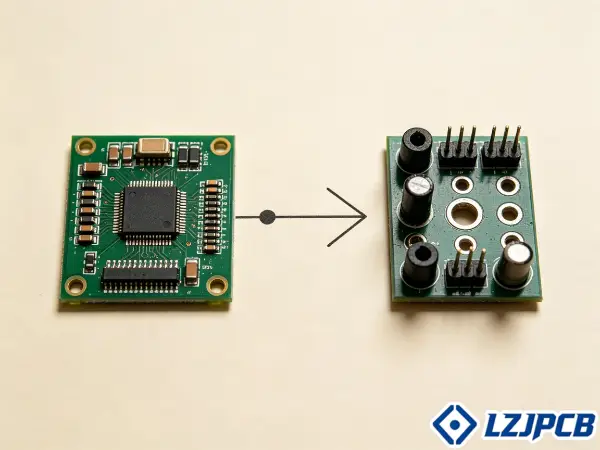
I make this call on every project. The right answer depends on your product, not on a rule. Below is the checklist I use with Medical Device PCB clients.
- What is your volume? Under 100 units leans through-hole. Over 1,000 leans SMT.
- How much power flows? High current and heavy heat lean through-hole or hybrid.
- How fast are your signals? Above 1 GHz needs SMT for shorter paths and lower parasitics.
- How small must the board be? Tight size needs SMT and its 60% space savings.
- Any heavy parts? Parts over 25–30 grams need through-hole for mechanical strength.
- What is the environment? High vibration needs through-hole or SMT with underfill.
Most boards land in the middle. That is why hybrid assembly is the industry norm, not the exception. I use SMT for dense digital logic and through-hole for connectors, transformers, and power devices.
A hybrid board follows a set sequence. We reflow the SMT parts first. Then we add through-hole parts. Then we wave solder or selectively solder those parts. This order protects the SMT joints from a second full heat cycle.
For industrial automation boards, this hybrid path fits well. The digital control section uses SMT for density and speed. The power and connector section uses through-hole for strength and current. This gives the reliability his market demands without wasting money.
My advice is direct. Do not force one technology onto the whole board. Split the design by function. Use each mount type where it wins. Then let a factory with both lines build it as one product.
FAQ About SMT Disadvantages
The most common SMT questions cover power limits, repair difficulty, reliability, and cost. Below I answer each in plain terms based on real project work.
Can SMT handle high-power circuits?
SMT handles moderate power with the right design. Use power SMDs with thermal pads and thermal vias. For very high current or heavy heat, use through-hole or a hybrid board. One SMT pin carries about 1–2A, far less than a through-hole lead.
Why is SMT rework so expensive?
SMT rework needs a hot-air station, a preheater, and skill. A pro station costs $5,000–$20,000. Parts sit close, so heat can damage neighbors and lift pads. Rework runs 3–5 times the cost of through-hole repair for the same part count.
Are SMT solder joints reliable?
SMT joints are reliable when designed and processed well. Mature lines hold defects below 50 ppm. But small joints fatigue under thermal cycling. For harsh use, add underfill for BGAs and test against IPC-9701 cycling ranges.
When is SMT cheaper than through-hole?
SMT gets cheaper as volume climbs. The crossover sits near 1,000 to 5,000 units. Below 100 units, through-hole often wins because SMT setup and stencil costs spread over too few boards.
Do I always need X-ray inspection for SMT?
You need X-ray for hidden joints like BGA and QFN. Their joints sit under the part, so no camera can see them. For visible joints, AOI is enough. I always X-ray BGA boards before shipping.
Can I mix SMT and through-hole on one board?
Yes, and most real boards do. Hybrid assembly uses SMT for dense logic and through-hole for power and connectors. We reflow SMT first, then add and wave-solder the through-hole parts. This is standard practice, not a compromise.
Conclusion
SMT trades power, easy repair, and cheap small runs for density and speed. Know these limits, design around them, and pick the right mount type per function.