Skip to content
A weak BMS main control PCB can damage the whole battery pack. One sensing error can trigger overcharge, deep discharge, or even thermal runaway.
A reliable automotive BMS main control PCB depends on 8 factors: cell voltage accuracy, high-reliability ICs, thermal stability, strong isolation, EMI robustness, redundant protection, precise current sensing, and vibration resistance. Each factor protects the battery pack and keeps it safe over many years.
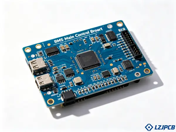
I have managed over 300 PCB projects, and BMS boards are some of the hardest. Let me walk you through what really matters.
How the BMS Main Control PCB Manages Battery Packs
A battery pack with no smart control is a fire risk. Cells drift, heat builds up, and no one knows until it fails. The BMS main control PCB is the brain that stops this.
The BMS main control PCB manages battery packs by reading cell data, controlling balancing, and cutting power during faults. It collects voltage, current, and temperature from cell monitor boards, then makes safety decisions to protect every cell.
The way the board does this comes down to three things: its core functions, how it talks to other boards, and how it keeps high voltage away from low voltage.
Core Functions of BMS Main Control PCBs in EV Battery Systems
The BMS main control PCB controls the whole battery system. Here are its core jobs:
- Read cell voltage at millivolt-level precision to stop overcharge and deep discharge.
- Measure current to calculate state of charge (SOC) and state of health (SOH).
- Track temperature across the pack to spot hot spots early.
- Control cell balancing to keep all cells at a similar charge.
- Trigger protection cutoffs during over-voltage, over-current, or over-temperature events.
- Store fault history and diagnostics for long-term traceability.
I always tell clients that cell voltage accuracy is the heart of it all. If the board reads voltage wrong by even a few millivolts, it can charge a cell too high or drain it too low. Both cause permanent damage. Battery systems also need records for many years, so the board must log fault data over its full life. This matters in automotive and energy storage use, where warranty claims can come years later.
Communication Interfaces Between BMS Main and Cell Monitor Boards
The main control PCB does not measure every cell by itself. It works with cell monitor boards spread across the pack. These boards must talk clearly and fast.
Common interfaces include:
| Interface | Use | Strength |
|---|---|---|
| CAN | Talk to the vehicle and other BMS nodes | Robust, noise-tolerant |
| RS-485 | Daisy-chain cell monitor links | Long distance, simple |
| SPI / Isolated SPI | Fast data from AFE chips | High speed, short range |
| Daisy-chain isolated links | Stack cell modules in series | Built-in isolation |
CAN and RS-485 are key for safety coordination across the vehicle. They let the BMS share state with the motor controller and charger. The link between the main board and cell monitors carries the most critical data. So I keep these traces short and shielded. Careful layout here keeps sensing stable even when high current flows nearby.
Isolation Design for High-Voltage Safety on BMS PCBs
A BMS board mixes two worlds. One side handles 400V or 800V battery stacks, and other side runs low-voltage logic at 3.3V or 5V. These must never touch.
This is where my first insight is firm: the BMS main control PCB must isolate high-voltage and low-voltage sections with strict creepage and clearance design. I use digital isolators, isolated power supplies, and clear keep-out zones on the board. I also add slots and cutouts in the copper to push creepage distance higher. High-Tg materials and multilayer builds help here too. They give better electrical safety and hold up under heat and stress. A good isolation barrier is what keeps a technician safe and stops a single fault from spreading across the system.
Voltage and Temperature Sensing Accuracy for BMS Main Control PCB
Bad sensing data leads to bad decisions. If the board misreads voltage or temperature, it may overcharge a cell or miss a hot spot. The cost is a dead pack or a fire.
Sensing accuracy on a BMS main control PCB depends on ADC resolution, a stable reference voltage, and clean thermistor circuits. Accurate voltage, current, and temperature readings must stay stable under high-current load to keep the battery reliable and safe.
Accurate sensing is central to battery reliability. Let me break down the three parts that decide how good your readings are.
ADC Resolution and Reference Voltage Stability on BMS PCBs
The ADC turns the cell voltage into a number the MCU can use. If the ADC is weak or the reference drifts, every reading is off.
Key points I check:
- Use high-resolution ADCs, often 16-bit or higher, for millivolt accuracy.
- Pick a low-drift voltage reference with tight temperature coefficient.
- Place the reference away from heat sources to avoid drift.
- Filter the ADC input to reject noise from switching power stages.
My third insight applies here. Thermal stability of the PCB design is essential, since temperature drift can distort sensing accuracy. So I use low-temperature-coefficient parts and plan clean thermal paths. A reference that shifts with heat will fake a voltage change that is not real. The board then balances or cuts power for no reason. Good ADC and reference design is the base for trustworthy SOC math.
Thermistor Interface Design for BMS PCB Temperature Monitoring
Temperature tells the board when a cell is in danger. Thermistors are cheap and common, but the interface must be done right.
I follow these steps:
- Use pull-up resistors with tight tolerance for a stable divider.
- Route thermistor lines away from high-current and switching traces.
- Add filtering to block noise on long sensor wires.
- Place sensors at known hot spots, not random points.
Thermal management is critical. Too much heat speeds up cell aging and can trigger thermal runaway. The board must see the rise early and act. A noisy or poorly placed thermistor circuit gives late or wrong data. That delay can be the difference between a safe shutdown and a fire. So I treat temperature sensing with the same care as voltage sensing.
Cell Balancing Control Signals From the BMS Main Control PCB
Cells never stay perfectly matched. Over time, some hold more charge than others. The main control PCB sends balancing signals to fix this.
Cell balancing is a core BMS function. It improves usable capacity, extends pack life, and reduces uneven degradation. The board can use passive balancing, which bleeds extra charge through resistors, or active balancing, which moves charge between cells. Either way, the control signals must be clean and well-timed. I keep these signal traces short and shielded so noise does not cause a wrong balance command. I also plan the thermal path, because balancing resistors makes heat. Good balancing control means the pack gives more range and lasts longer. It is one of the clearest ways a BMS adds value.
How to Select Automotive-Grade Components for BMS Main Control PCB
A consumer-grade part on a car battery board is a gamble. It may fail in heat, vibration, or after a few years of stress. In an EV, that failure is not just annoying. It is dangerous.
Automotive-grade BMS components must be AEC-Q100 qualified ICs, vibration-resistant connectors, and properly derated passives. These parts survive heat, shock, and continuous electrical stress inside EV battery packs, which keeps the board reliable over its full service life.
High-reliability IC selection is critical because BMS boards run nonstop under high stress. Let me show you what to pick and why.
AEC-Q100 Qualified ICs for BMS Main Control PCB
The main ICs are the battery monitor chip, the AFE, and the MCU. These do the real work, they must be built for car use.
I look for these traits:
- AEC-Q100 qualification for the full automotive temperature range.
- Built-in diagnostics for fault detection inside the chip.
- Wide operating voltage to handle pack-level swings.
- Long-term supply support, since car programs run for years.
The AFE and battery monitor IC must keep cell voltage accuracy at the millivolt level. The MCU must run safety logic with no glitches. These chips face high electrical stress all day, so consumer parts will not last. I source from trusted lines like TI, Infineon, ADI, and NXP, all backed by genuine, traceable channels. A qualified IC costs more up front. It saves far more by avoiding field failures.
Connector Selection for Vibration Resistance on BMS PCB
A BMS board lives inside a moving car. It shakes all day and goes through hot and cold cycles. Connectors are a common weak point.
I choose connectors with these features:
- Locking latches that resist vibration loosening.
- Gold-plated contacts for low resistance over time.
- High mating cycle ratings for service work.
- Sealed types where moisture is a risk.
Mechanical and vibration resistance is necessary, since the board sits inside a pack exposed to constant shaking, shock, and thermal cycling. A loose connector breaks sensing or comms at the worst time. So I match the connector to the real environment, not just the schematic. I also plan the footprint and strain relief on the board itself. A strong solder joint with a weak connector still fails. The whole path must hold.
Passive Component Derating for BMS Main Control Boards
Resistors and capacitors look simple, but they fail too if pushed too hard. Derating means running a part below its rated limit. This adds margin and life.
My derating rules of thumb:
| Component | Stress | Typical Derating |
|---|---|---|
| Resistor | Power | Use 50% of rated power |
| Capacitor | Voltage | Use 50% of rated voltage |
| MLCC | Temperature | Stay below max temp range |
| Connector | Current | Use 70% of rated current |
Passive derating is a quiet but powerful reliability tool. A capacitor running near its full voltage rating ages fast and may short. On a high-voltage BMS board, that short can be a safety event. So I always leave headroom. I also pick automotive-rated passives with stable temperature behavior. This ties back to thermal stability, since stable passives keep sensing and timing accurate. Derating is cheap insurance for a board that must run for a decade.
BMS Main Control PCB Cost Drivers: From NPI to High-Volume
Cost surprises kill projects. Many buyers see a low prototype price, then face a high mass-production bill. With BMS boards, you must understand the drivers early.
The main cost drivers for a BMS main control PCB are layer count, board size, surface finish, and test fixtures. These set the price at both the new product stage and high volume, so plan them with reliability in mind, not just cost.
I help clients balance cost and reliability every week. Here is where the money really goes.
Layer Count and Board Size Impact on BMS Main Control PCB Pricing
Layers and size are the biggest base cost drivers. More layers and bigger boards cost more, but they often bring reliability you cannot skip.
How they affect cost:
- More layers raise material and process cost per board.
- Larger boards use more panel space, so fewer fit per panel.
- HDI and blind or buried vias add steps and cost.
- Tight impedance control adds testing and process care.
For BMS boards, multilayer builds are not a luxury. They give clean isolation between high and low voltage. They also support EMI control with solid ground planes. My eighth insight matters here: careful layout and EMI reduction keep sensing and comms stable. A board crammed into too few layers may cost less but fail in the field. I help clients find the layer count that meets safety needs at the lowest real cost. At LZJPCB, we build 1 to 32 layers in mass production, so we can scale with your design.
High-Reliability Surface Finish Options for BMS PCBs
The surface finish protects the copper pads and sets solder quality. For automotive use, the finish must hold up for years.
Common options and trade-offs:
| Finish | Reliability | Cost | Best For |
|---|---|---|---|
| ENIG | High, flat surface | Medium-high | Fine pitch, long life |
| Immersion Silver | Good | Medium | High frequency |
| Lead-free HASL | Fair | Low | Simple, low-cost boards |
| ENEPIG | Very high | High | Critical, wire bond |
For BMS main control boards, I usually recommend ENIG. It gives a flat surface for fine-pitch ICs and resists corrosion well. That corrosion resistance matters because the board faces moisture and contaminants in a vehicle. A cheaper finish may save a little now and cost a recall later. The finish is a small part of total cost but a large part of long-term reliability.
Test Fixture and ICT Costs for BMS Main Control Boards
Testing is where many buyers underbudget. A safety-critical board needs full testing, and that needs fixtures and time.
Test costs include:
- ICT fixtures to check every node on the board.
- Functional test rigs that mimic real battery behavior.
- AOI and X-ray for hidden joints under BGAs.
- Long-duration reliability testing before release.
A reliable BMS process must include performance testing, long-duration reliability testing, and iterative validation before release. This is not optional for a board that protects a battery pack. The fixture cost spreads across volume, so it hurts less at scale. At LZJPCB, we run 100% electrical test plus AOI, and add X-ray for BGA joints. I tell clients to plan test cost from day one. A board that ships untested is a risk no one can afford.
6 Standards That Validate BMS Main Control PCB Reliability
Words like "high quality" mean nothing without proof. Standards give that proof. They turn a claim into a tested, measured result that an auditor can check.
Six key standards validate BMS main control PCB reliability: ISO 26262 ASIL-D for functional safety, IPC-6012DA automotive addendum for fabrication, and environmental tests like thermal shock and humidity. Together they confirm the board is safe for automotive battery use.
Michael, my typical client, always asks for certs first. Here is what each standard proves.
ISO 26262 ASIL-D for BMS Main Control PCB Functional Safety
ISO 26262 is the road vehicle functional safety standard. ASIL-D is its highest risk level. A BMS that can cause a fire sits at this level.
What ASIL-D demands:
- Redundant protection paths in hardware and software.
- Fault detection and safe shutdown within set time limits.
- Full documentation of safety goals and design choices.
- Validation that the board reaches a safe state on failure.
My sixth insight fits here: redundant protection for over-voltage, under-voltage, over-current, and thermal cutoff is essential. ASIL-D forces this redundancy. So if one path fails, another still protects the pack. This is why I plan both hardware cutoffs and software checks. A board that meets ASIL-D thinking is far harder to push into a dangerous state. It is the backbone of BMS safety design.
IPC-6012DA Automotive Addendum for BMS PCB
IPC-6012 sets rules for rigid PCB quality, and DA addendum adds automotive-specific demands. It raises the bar for boards in cars.
This standard covers:
- Tighter copper plating and hole wall quality rules.
- Stronger thermal cycling survival requirements.
- Class 3 level inspection for high-reliability boards.
- Material and build checks for harsh use.
My ninth insight is direct: automotive BMS PCBs typically need IPC-A-600 and IPC-6012 Class 3 standards with strict SMT process control. The DA addendum builds on this for car use. At LZJPCB, we hold IATF16949, the automotive PCB quality standard, plus ISO9001 and UL. So we build BMS boards to the right class with traceable materials. Meeting IPC-6012DA shows the board can survive years of thermal and mechanical stress.
Environmental Testing: Thermal Shock and Humidity for BMS Boards
A lab-perfect board still has to survive the real world. Environmental tests prove it can. They push the board through hot, cold, and wet conditions.
Key tests include:
| Test | What It Checks | Why It Matters |
|---|---|---|
| Thermal Shock | Fast hot-cold swings | Solder and via cracking |
| Humidity | Long damp exposure | Corrosion, leakage |
| Thermal Cycling | Repeated heat cycles | Joint fatigue over life |
| Vibration | Constant shake | Connector and joint failure |
Automotive BMS boards need strong resistance to vibration, moisture, and contaminants. These tests prove that resistance. Thermal shock finds weak solder joints and vias fast. Humidity testing finds corrosion and leakage paths that hurt isolation. I use low-CTE construction and high-Tg materials so the board passes these tests. A board that survives them in the lab will survive the road.
BMS Main Control PCB Production: 5 Pitfalls That Compromise Safety
A good design can still fail in production. Small process mistakes can break safety in ways no one sees until the field. I have seen these traps hurt real projects.
The biggest production pitfalls for BMS main control PCBs are creepage and clearance underspecification, weak thermal runaway containment, and poor conformal coating. Each one can compromise high-voltage safety, so strict process control during fabrication and assembly is essential.
Let me walk through the three traps I watch for most closely on every BMS build.
Creepage and Clearance Underspecification for High-Voltage BMS PCB
Creepage is the distance across the surface between conductors. Clearance is the distance through air. On a high-voltage BMS board, too little of either causes arcing.
Common mistakes I catch:
- Spacing set for low voltage, not the real pack voltage.
- No slots or cutouts to extend creepage in tight areas.
- Conformal coating is used as an excuse to shrink spacing.
- Dirty or contaminated surfaces that lower real creepage.
My fourth insight is strict here: strong isolation and creepage design is required for 400V or 800V packs. Underspec spacing is one of the most dangerous BMS errors. So I set spacing for the worst-case voltage, then add margin. I add board slots to push creepage higher without growing the board. This trap is silent until the day an arc forms. Then it is too late.
Thermal Runaway Containment on BMS Main Control Boards
Thermal runaway is the worst battery event. One cell overheats, then heat spreads to others. The BMS must help stop or slow this.
Steps for good containment:
- Place temperature sensors near known hot spots.
- Plan fast cutoff paths to drop the load quickly.
- Use thermal relief and copper planes to spread heat.
- Keep sensitive parts away from high-power zones.
Thermal management is critical, since excess heat speeds cell degradation and can trigger runaway. The board cannot stop running away alone, but it can detect it early and cut power fast. So I design clean thermal paths and place sensors with care. I also keep the MCU and AFE away from heat sources so their readings stay true. Poor thermal design lets a small fault grow into a fire. Good design buys the system time to react.
Conformal Coating Application for BMS PCB Environmental Protection
Conformal coating is a thin layer that protects the board from moisture, dust, and contaminants. On a car BMS, it is often a must. But poor coating causes its own problems.
Coating pitfalls and fixes:
- Thin or missing coverage near tall parts leaves gaps.
- Coating over the connector blocks contact, so mask them.
- Bubbles trap moisture instead of blocking it.
- Wrong cure time leaves a soft, weak film.
Automotive BMS boards face moisture and contaminants every day. A good conformal coating keeps these out and protects the isolation for years. But coating must never replace proper creepage design. I treat it as one layer of defense, not the only one. At LZJPCB, we control coating in a clean process with inspection. Done right, it adds real life to a board in a harsh vehicle environment. Done wrong, it hides a fault that grows over time.
Conclusion
A reliable automotive BMS main control PCB needs accurate sensing, strong isolation, automotive-grade parts, proven standards, and clean production. LZJPCB delivers all of this turnkey.